First Round Open Source 55nm Tapeout Results: Multiple Chips Successfully Brought Up!
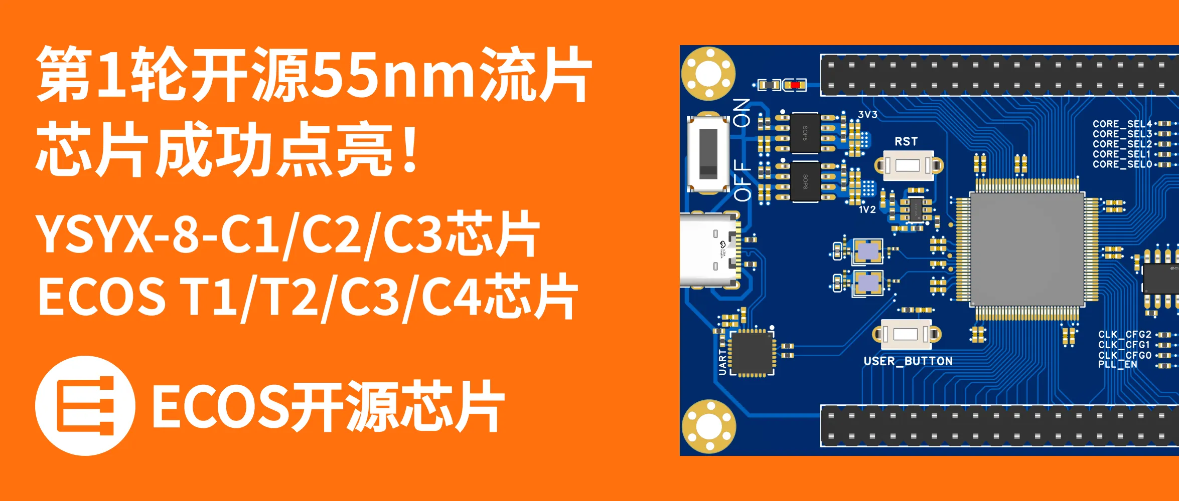
The ECOS Team and community users conducted comprehensive testing of the chips from the first open-source 55nm shuttle run, and several chips were successfully brought up. This marks the ECOS Team's transition from a solution that primarily served its own chip designs to an open platform that supports different types of users in developing small-batch chips, based on open-source EDA, open-source IP, and an open-source PDK.
01 Summary and Overview
In mid-July 2026, after the chips from the first ICS 55nm shuttle run had been packaged, the ECOS Team immediately organized engineers to test them and achieved encouraging results. At the same time, the team shipped the chips designed and taped out by five community users to the users themselves (packaged chips for digital designs and bare dies for analog designs). After designing, fabricating, and debugging their PCBs, three users have returned test results, while two have not yet started testing. The details are as follows:
-
Results from the first round of open-source tapeouts. The ECOS Team and open-source community users have completed the design, tapeout, and testing of multiple chips based on the ICsprout 55nm open-source PDK. These designs cover processor cores, SoCs, memory, PLLs, interface controllers, and AI accelerators. The test results show that several chips have passed core functional verification; ECOS T1 successfully verified PLL frequency multiplication and division for the first time.
-
ECOS open-source macro library. The ECOS open-source macro library is an important part of ECOS Factory. It provides silicon-validated, directly integrable IP packages, including SRAM Compiler, ROM Compiler, PLL, and other key IP types. Every macro IP package includes the corresponding LEF, Liberty, and Verilog models, as well as interface documentation. Users can configure and download SRAM and ROM macros online, greatly improving design efficiency and tapeout success rates.
02 First Round Tapeout Results
The YSYX-8-C1 through C3 chips were designed and tested by the ECOS Team. C1 integrates four "One Student One Chip" processor cores and one shared SoC, while C2 and C3 each integrate 13 "One Student One Chip" processor cores and one shared SoC. The processor core currently used for bring-up and functional verification (Phase B of "One Student One Chip") uses a pipelined architecture, supports the standard RV32E instruction set, and includes a cache to improve instruction and data access efficiency. The SoC integrates common IP modules such as UART, SPI, and GPIO, providing a relatively complete embedded-system runtime environment. With the current processor-core and SoC combination, the chips should be able to run relatively complex applications such as the RT-Thread real-time operating system and GUI-based games, while also supporting demonstration programs written by students. Note: C1 is functionally identical to C2 and C3; the difference is that its backend was implemented using a flat flow.
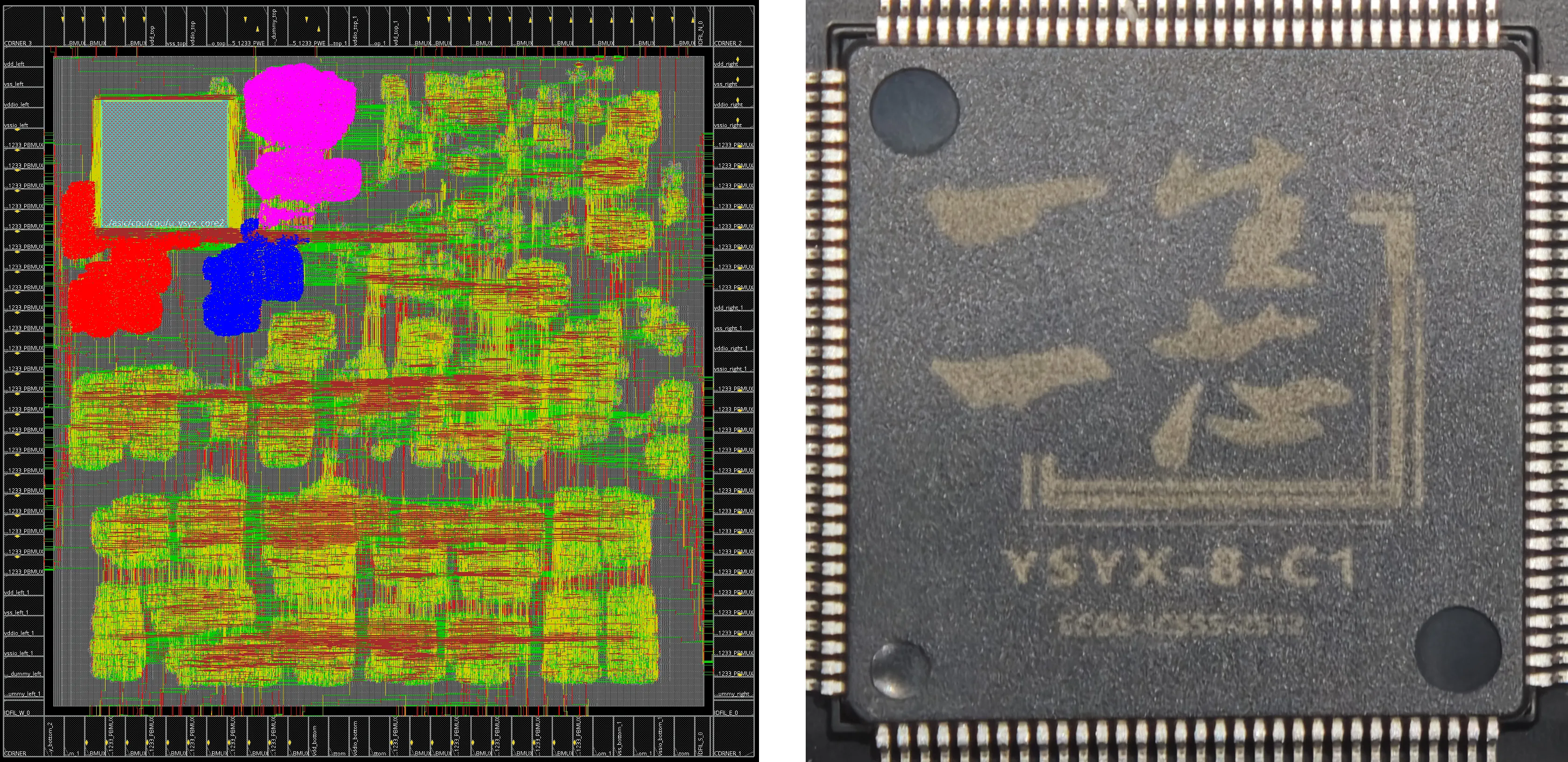
YSYX-8-C1 chip (tapeout ID: SoC3)
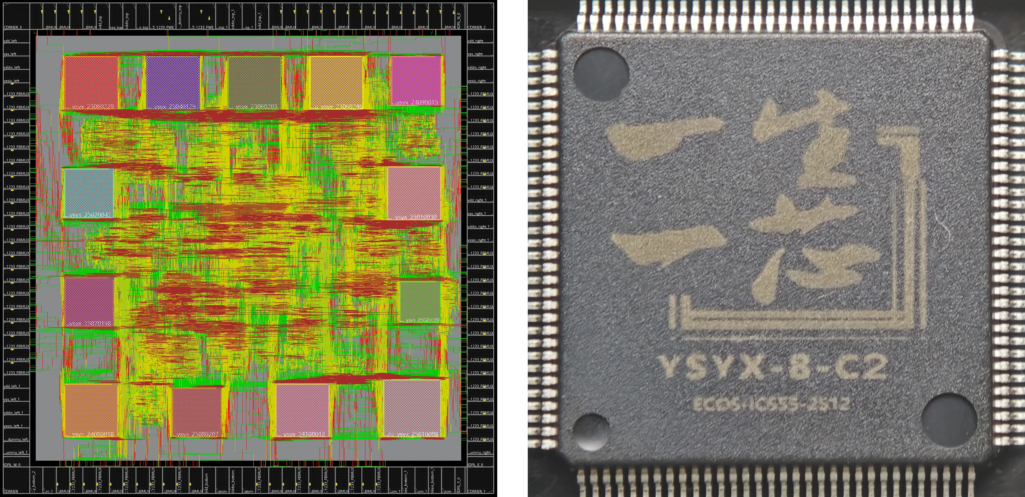
YSYX-8-C2 chip (tapeout ID: SoC1)
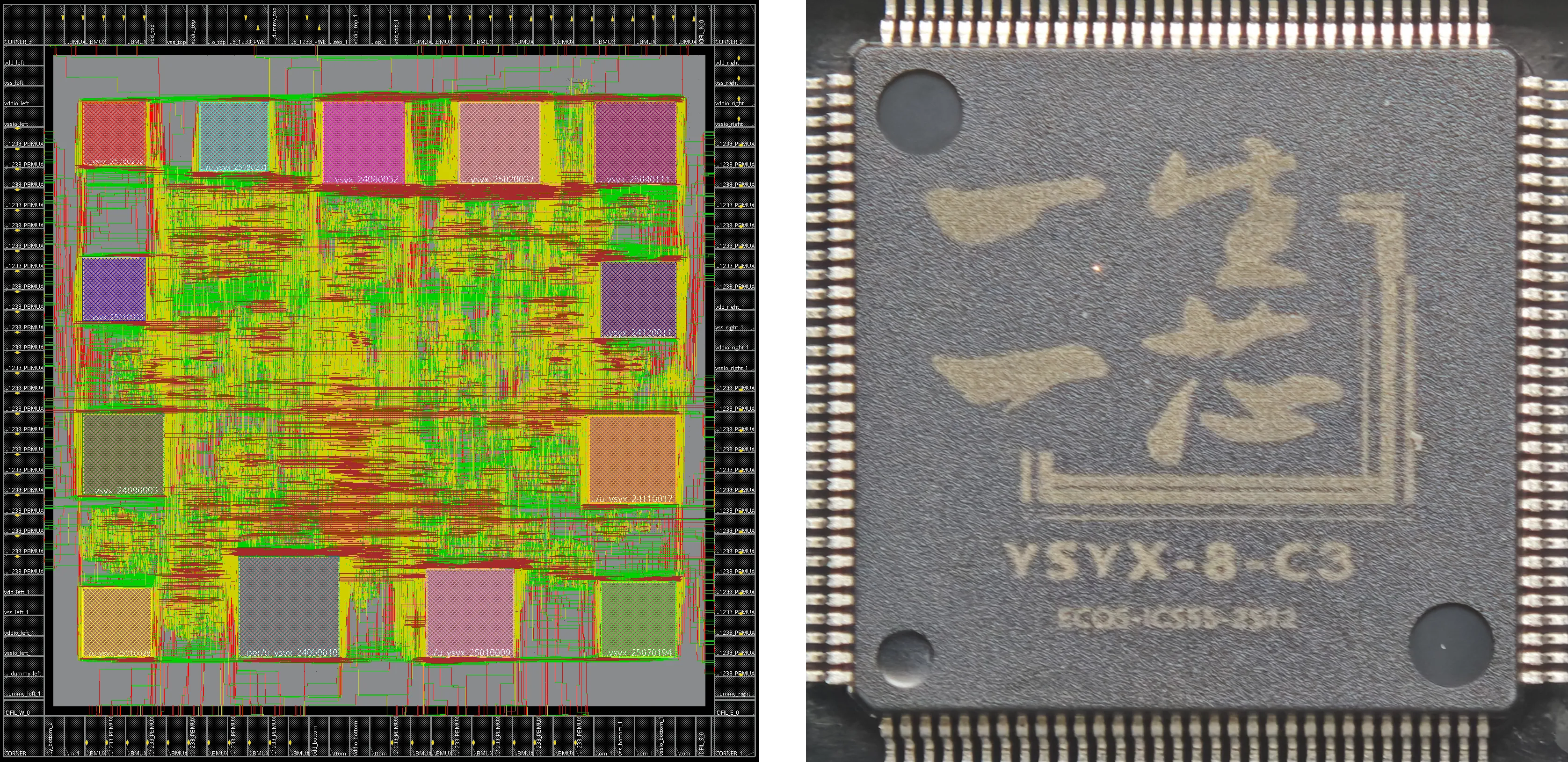
YSYX-8-C3 chip (tapeout ID: SoC2)
Testing of the YSYX-8-C1 through C3 chips covered the PSRAM, GPIO, PWM, TIMER, UART1, I2C, RNG, CRC, and QSPI IP modules. PSRAM was used to verify external-memory access and data read/write capability; GPIO, PWM, and TIMER verified general-purpose I/O, pulse-width modulation, and timer functions, respectively; RNG and CRC verified random-number generation and data-checking capability; and QSPI tested a high-speed serial interface and related memory access. After board-level testing, all test items have passed except for abnormalities in UART1 and I2C on the C2 and C3 chips. This indicates that the chips are generally functioning correctly, with the processors, memory systems, and most on-chip peripherals operating stably.
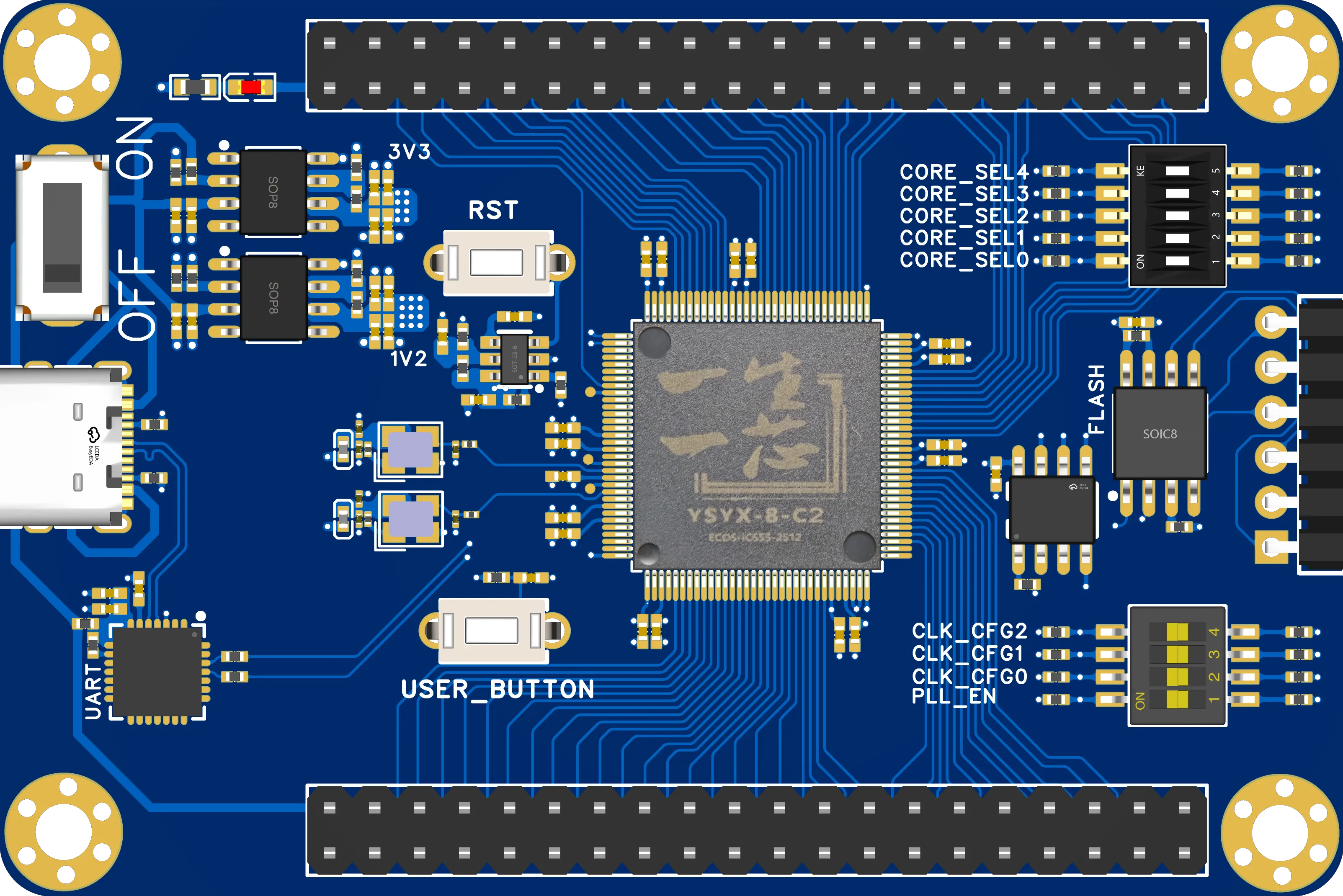
YSYX-8-C1 through YSYX-8-C3 chip board (test board)
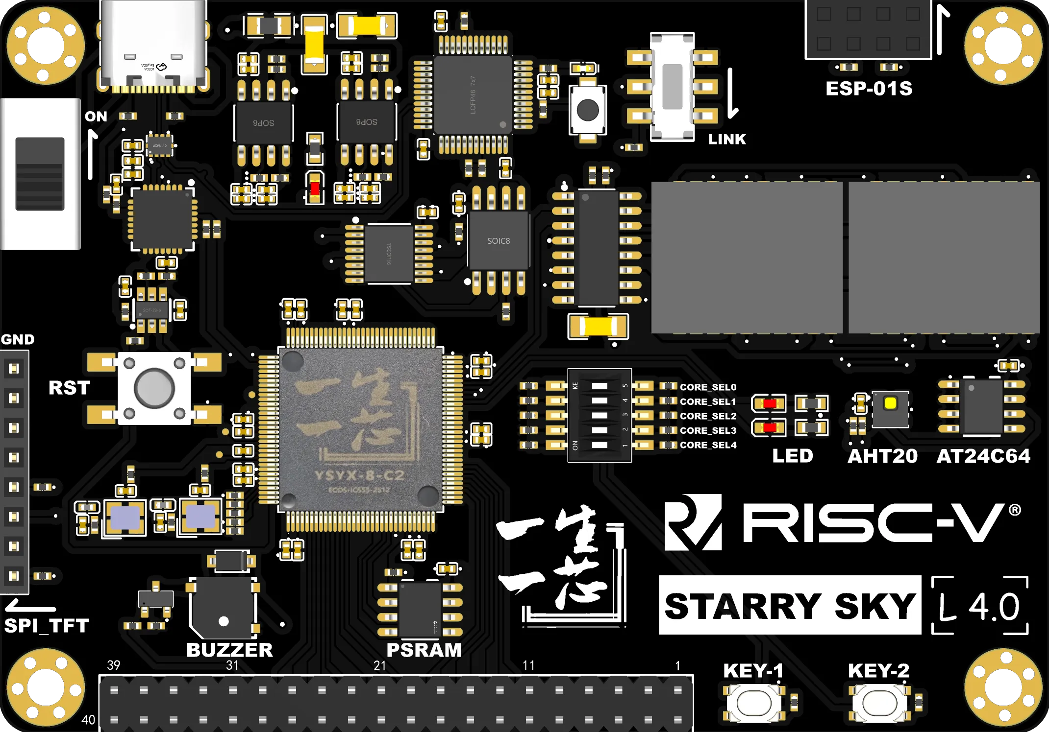
YSYX-8-C1 through YSYX-8-C3 chip board (StarrySky L4)
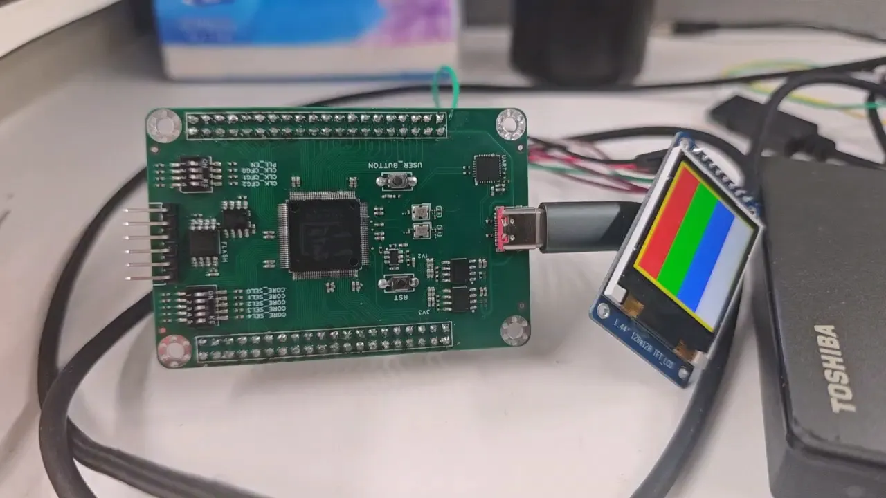
YSYX-8-C2 chip driving a QSPI color display (test board)
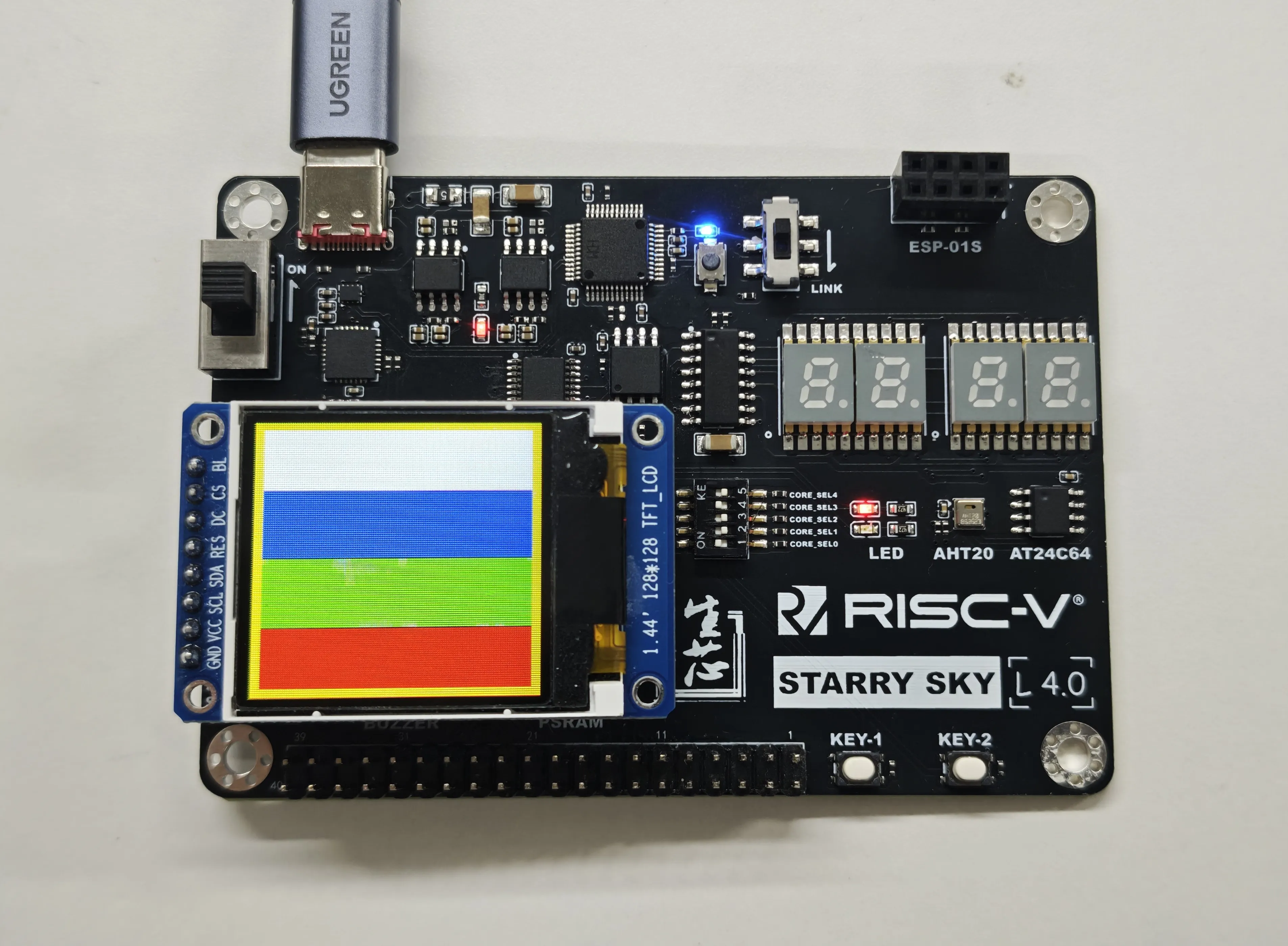
YSYX-8-C2 chip driving a QSPI color display (StarrySky L4)
The ECOS T1 and T2 chips were designed and tested by the ECOS Team. T1 uses an architecture combining an in-house CL1 processor core with a custom SoC, and is primarily intended to verify the ECOS Team's CL1 processor core and PLL. T2 serves as a control group for standalone PLL verification. The T1 CL1 processor core uses a pipelined architecture, supports the standard RV32IMC instruction set, and includes a cache to improve memory-access efficiency while retaining flexible instruction execution. The custom SoC integrates multiple IP modules, including UART, SPI, GPIO, I2C, PLIC, SDRAM, and JTAG. It also introduces, for the first time in a 55nm open-source chip, a PLL with fully independent intellectual property, capable of clock multiplication and division to provide stable and reliable clocks for the processor core and functional modules.
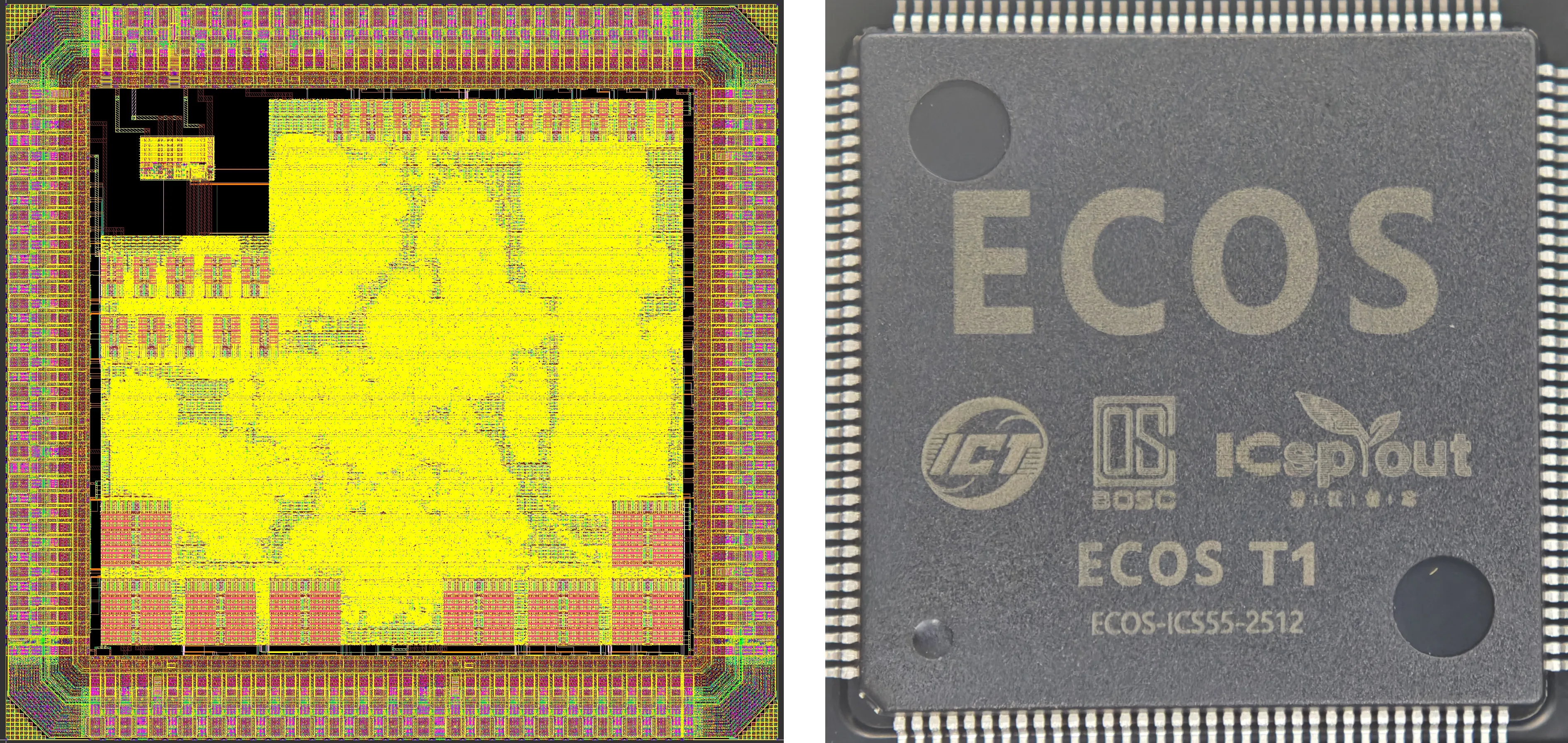
ECOS T1 chip (tapeout ID: SoC6)
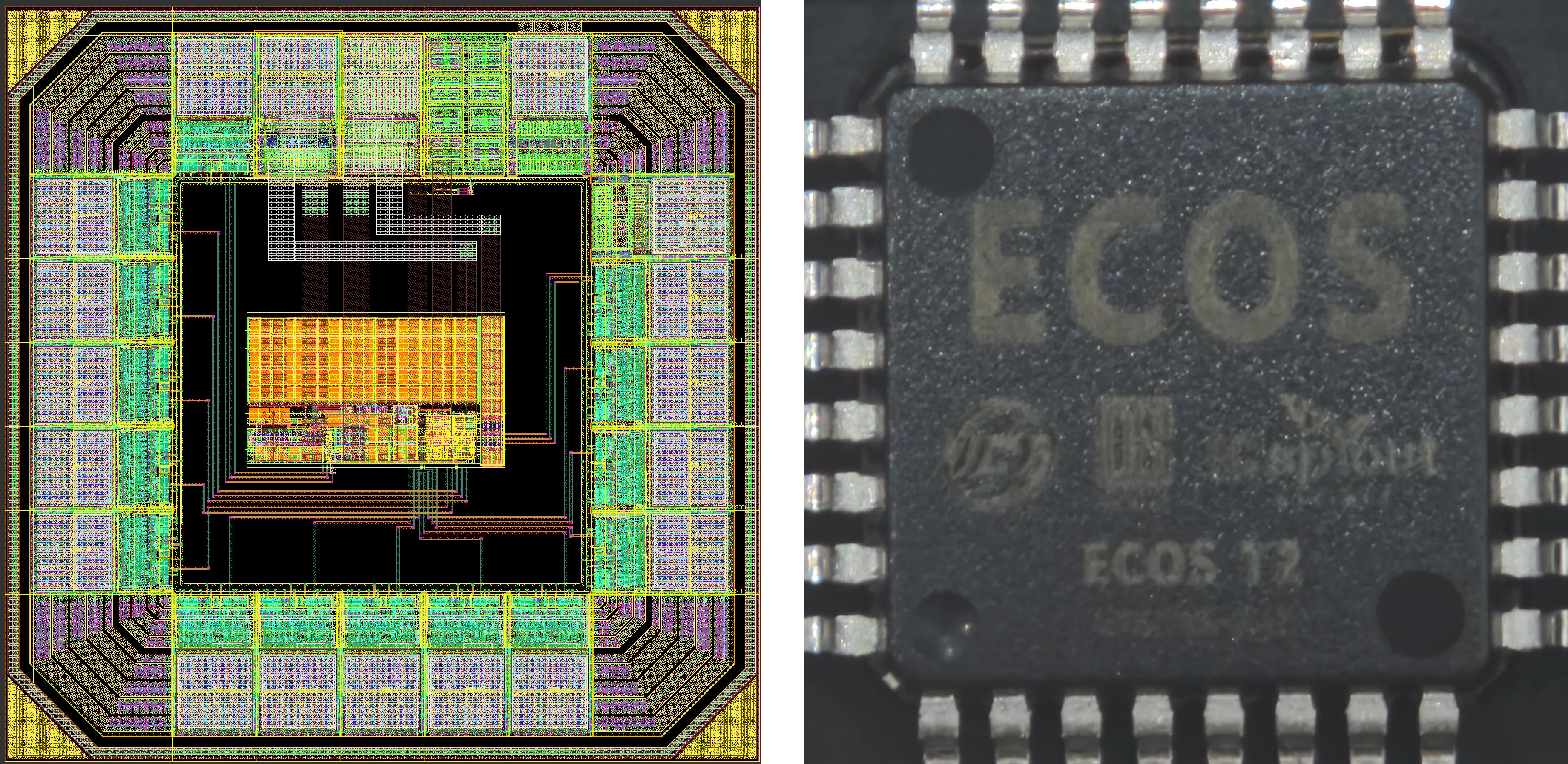
ECOS T2 chip (tapeout ID: Ana1)
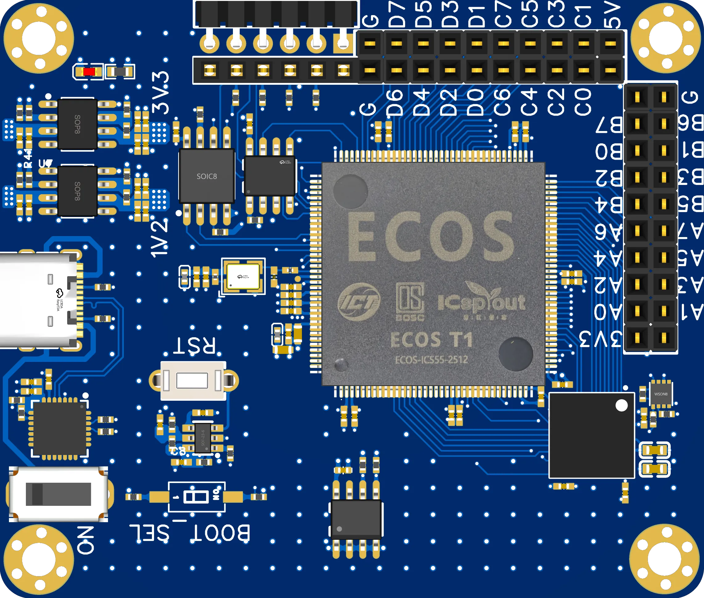
ECOS T1 chip board (test board)
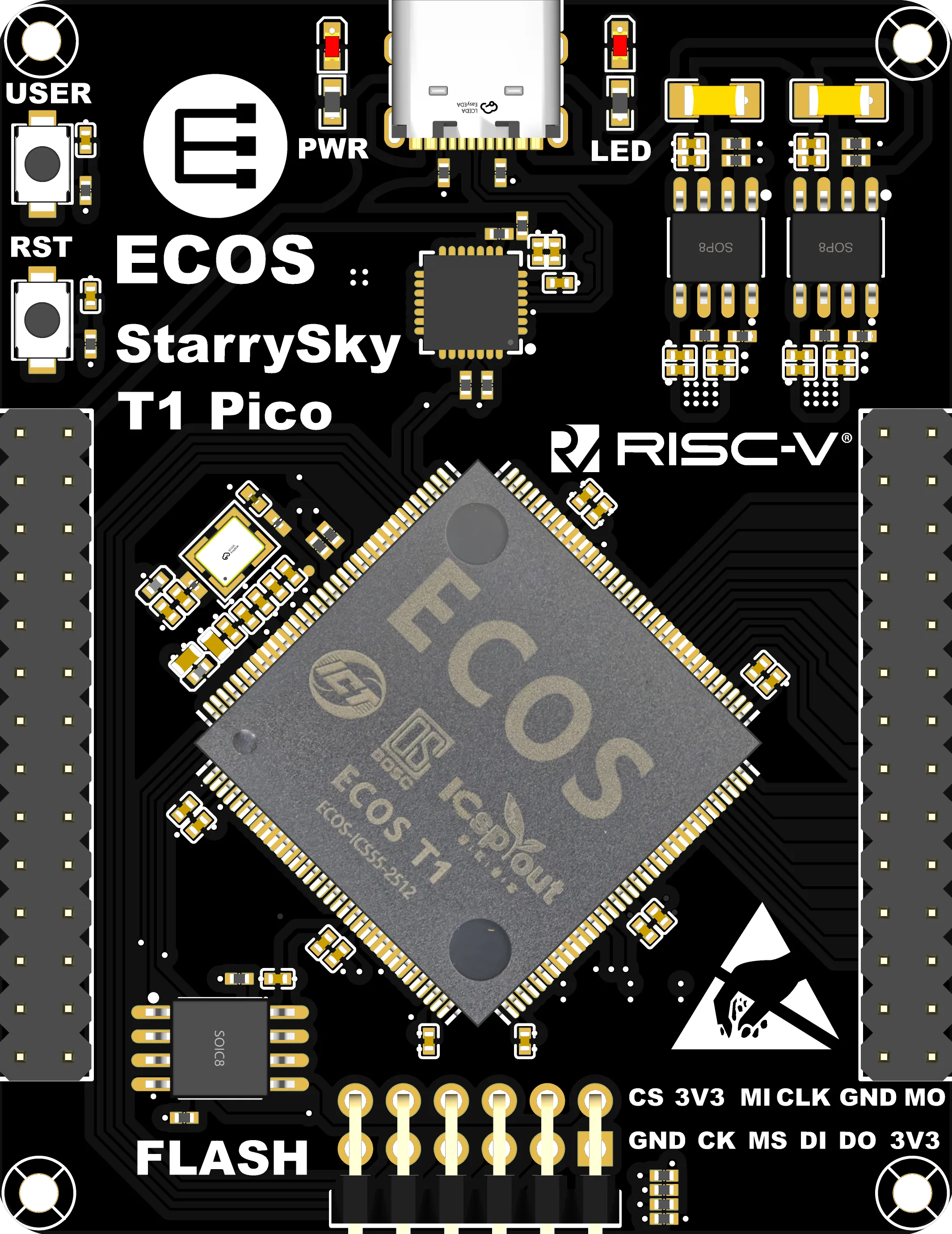
ECOS T1 chip board (StarrySky T1 Pico)
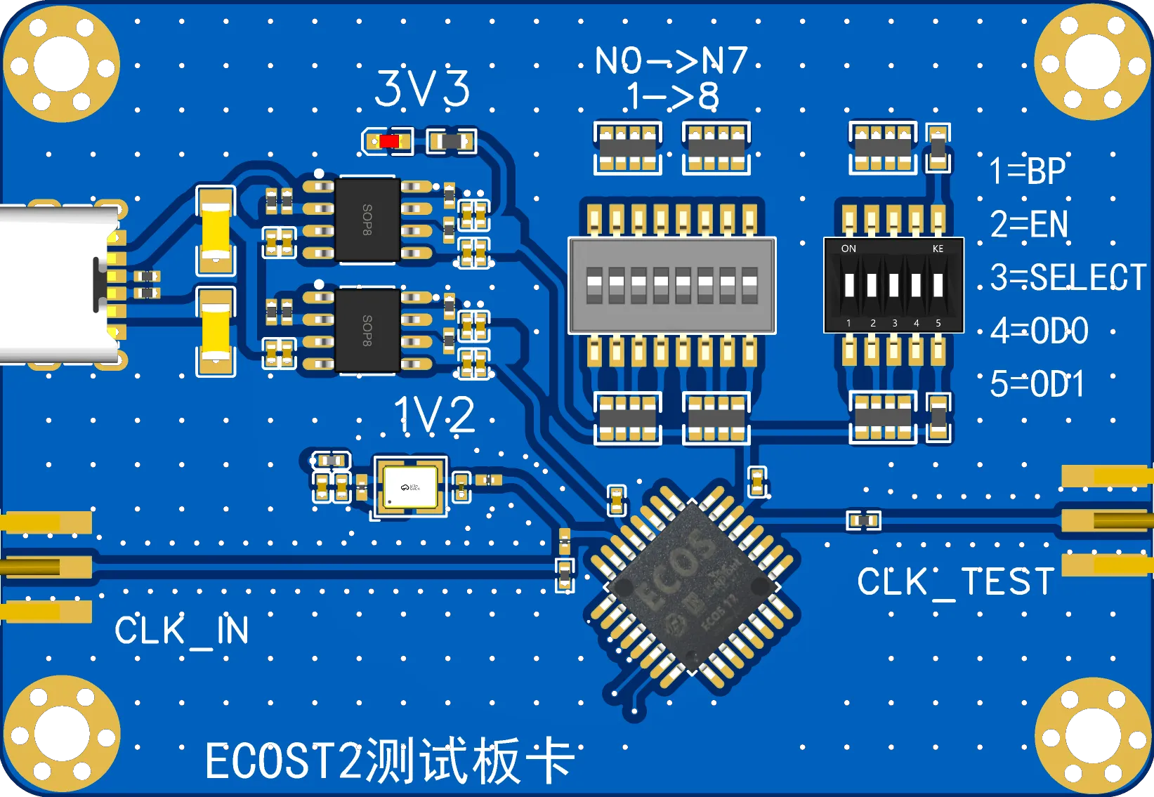
ECOS T2 chip board
Testing of the ECOS T1 chip focused on the PLL, ISRAM, I2C EEPROM, QSPI PSRAM, CLINT, GPIO, SDRAM, PLIC, timer interrupt, and JTAG IP modules, while testing of T2 covered only the PLL. The results show that the PLLs on both chips operated correctly, successfully generating the expected 100 MHz and 50 MHz divided clocks with an eightfold divider; the measured waveforms matched expectations. This means that users may be able to use this PLL as soon as the ECOS Team's next 55nm shuttle run. The team also paid particular attention to T1's JTAG module and confirmed that the chip has basic online debugging capability, laying a solid foundation for testing the remaining IP modules. Ultimately, ECOS T1 and T2 passed all test items and met the expectations set before tapeout.
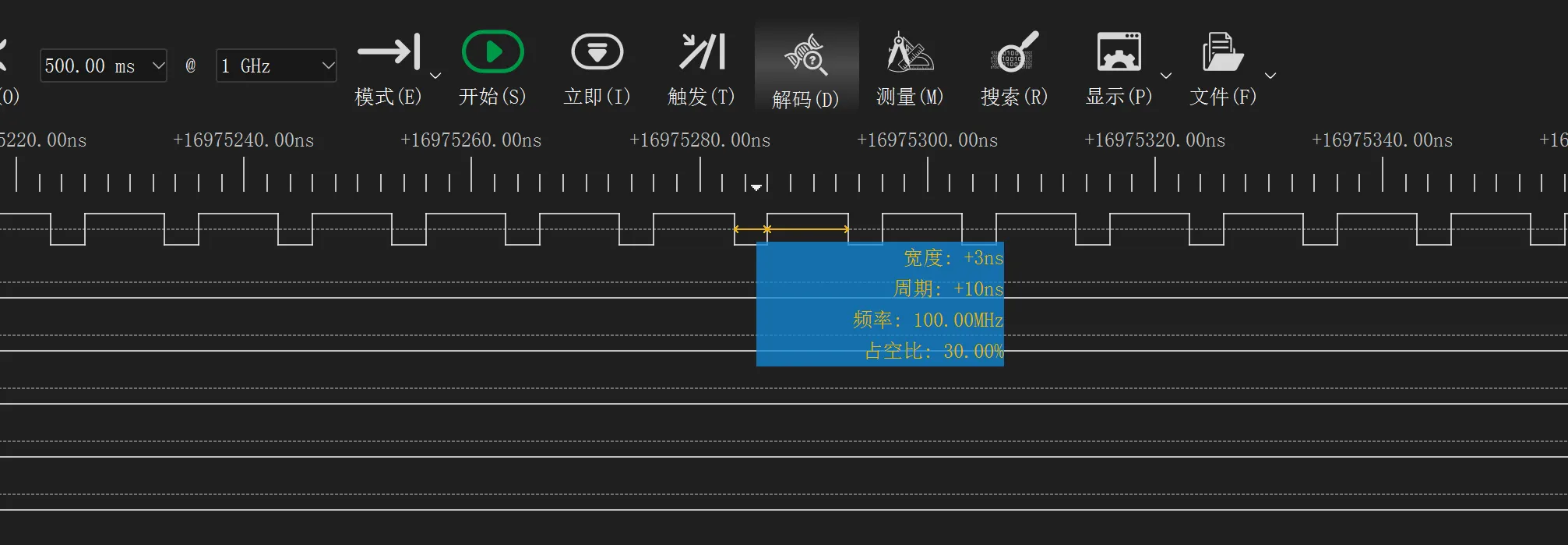
100 MHz divided clock output from the PLLs on ECOS T1 and T2
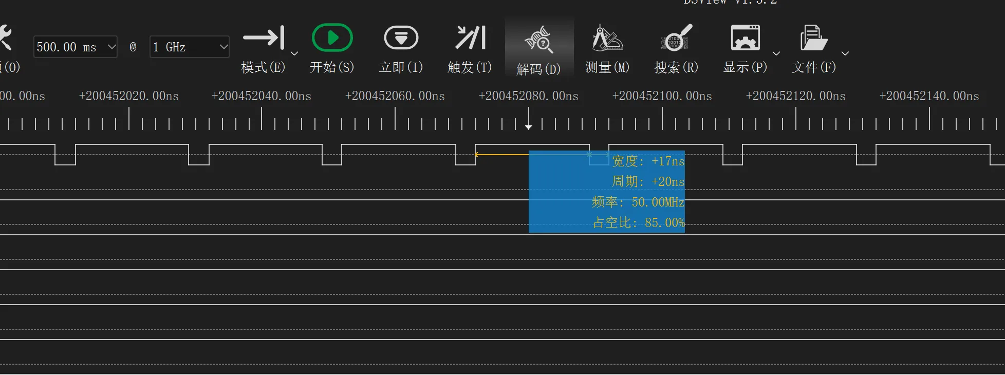
50 MHz divided clock output from the PLLs on ECOS T1 and T2
The ECOS C3 chips were tested by community user Xiaoyu Hong and the Xiaojun Tong team, respectively. Xiaoyu Hong's chip is a VexRiscv-based MCU that supports the RV32IM instruction set and uses a five-stage pipeline. It communicates with a serial port, PWM, SPI Flash, and an LPC bus through an AHB bus, and supports clock and external interrupts. The Xiaojun Tong team's chip is a Chisel-based RISC-V AI accelerator. It uses a PicoRV32 processor core (RV32I), communicates with CompactAccel (an 8x8 matrix accelerator) and BitNetAccel (an 8x8 multiplier-free accelerator) through a simplified register interface, and supports UART, GPIO, and interrupt control for edge AI inference.
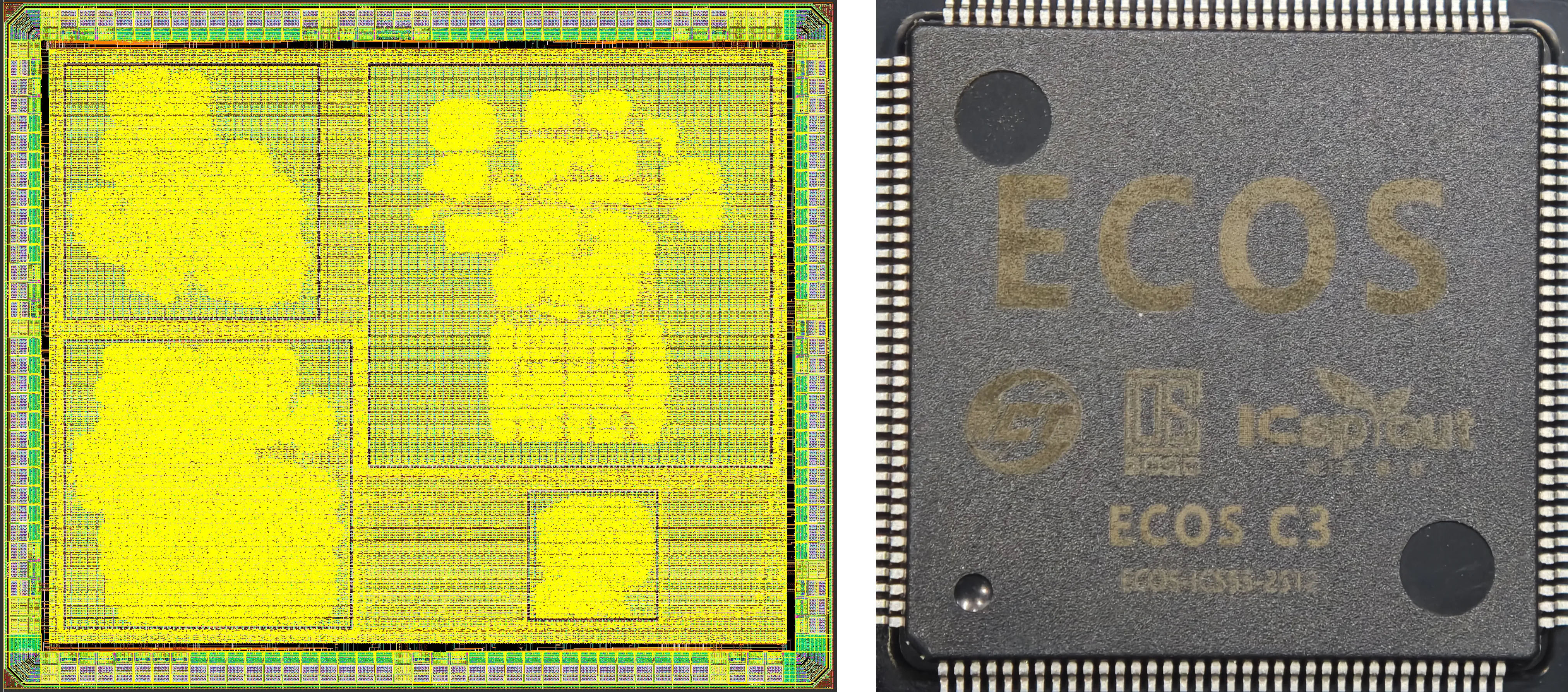
ECOS C3 chip (tapeout ID: SoC4)
Xiaoyu Hong's chip test results were as follows: the chip was successfully brought up, and its clock, reset, and JTAG connections were normal; OpenOCD could read the JTAG ID and perform CPU debugging, and mcycle, the on-chip 1 KiB SRAM, APB peripherals, and external SRAM read/write operations all passed; and test programs for the on-chip and external SRAM ran successfully. Dhrystone was generally normal, although timer support has not yet been ported. CoreMark produced abnormal jumps and stack corruption, initially attributed to differences in SRAM timing between the FPGA and ASIC. RT-Thread failed to boot because the mscratch register was not configured. The next steps are to add SRAM wait cycles and complete RT-Thread adaptation and verification using an alternative approach.
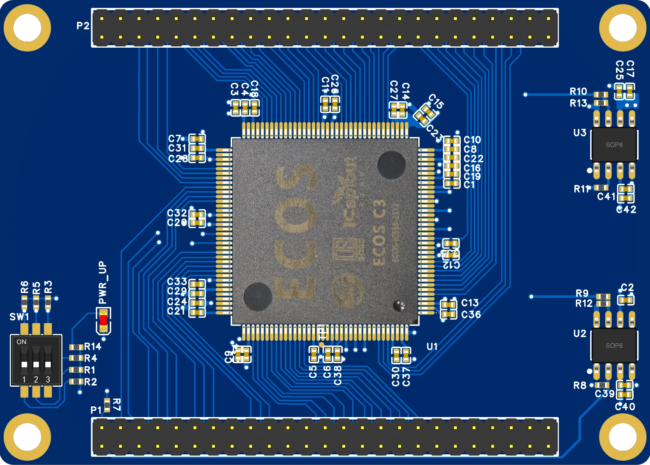
ECOS C3 chip board (Xiaoyu Hong)
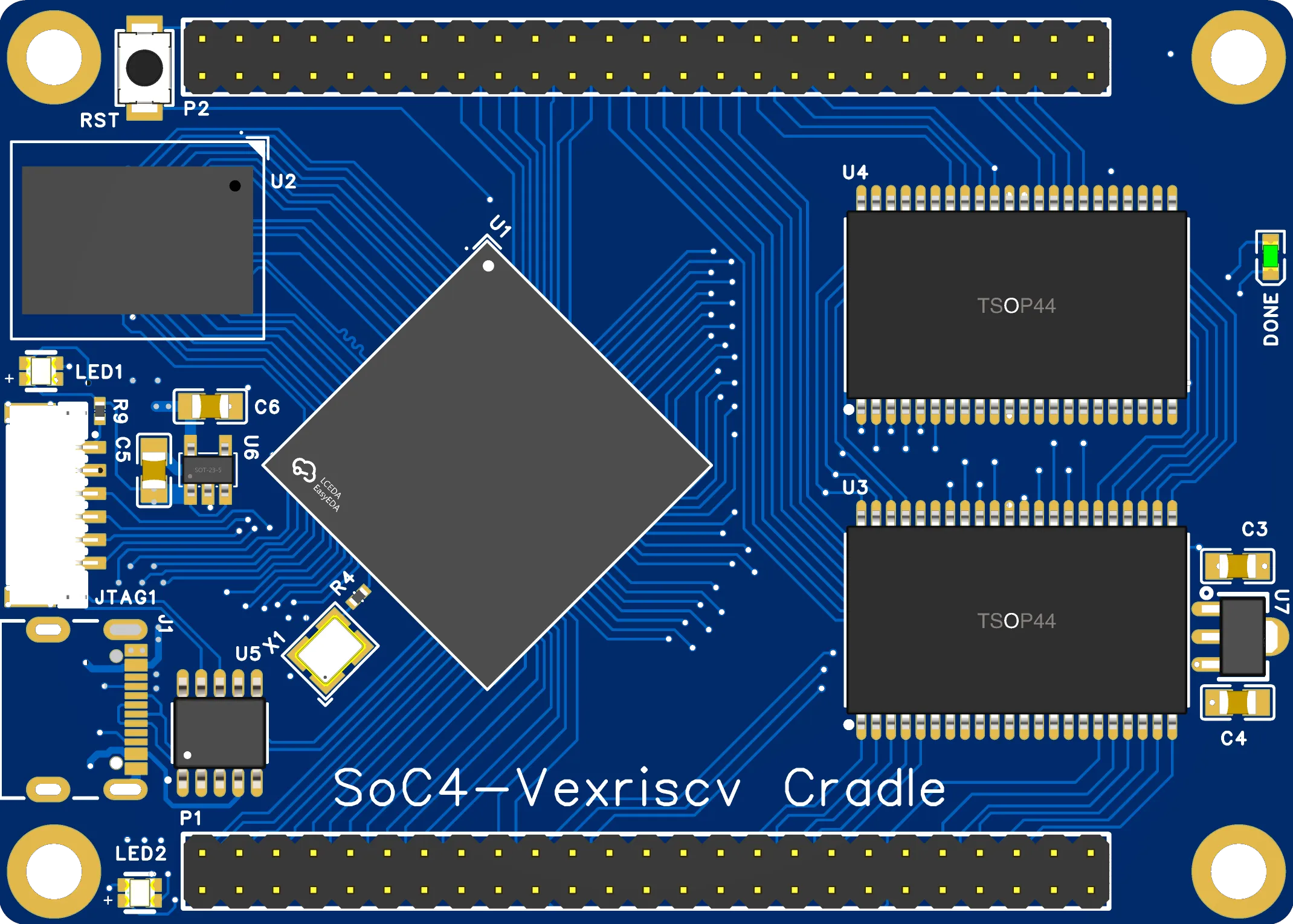
FPGA minimal system board (Xiaoyu Hong)
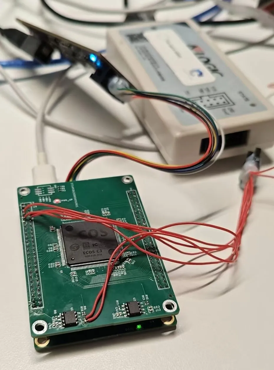
ECOS C3 chip board and FPGA board assembly (Xiaoyu Hong)
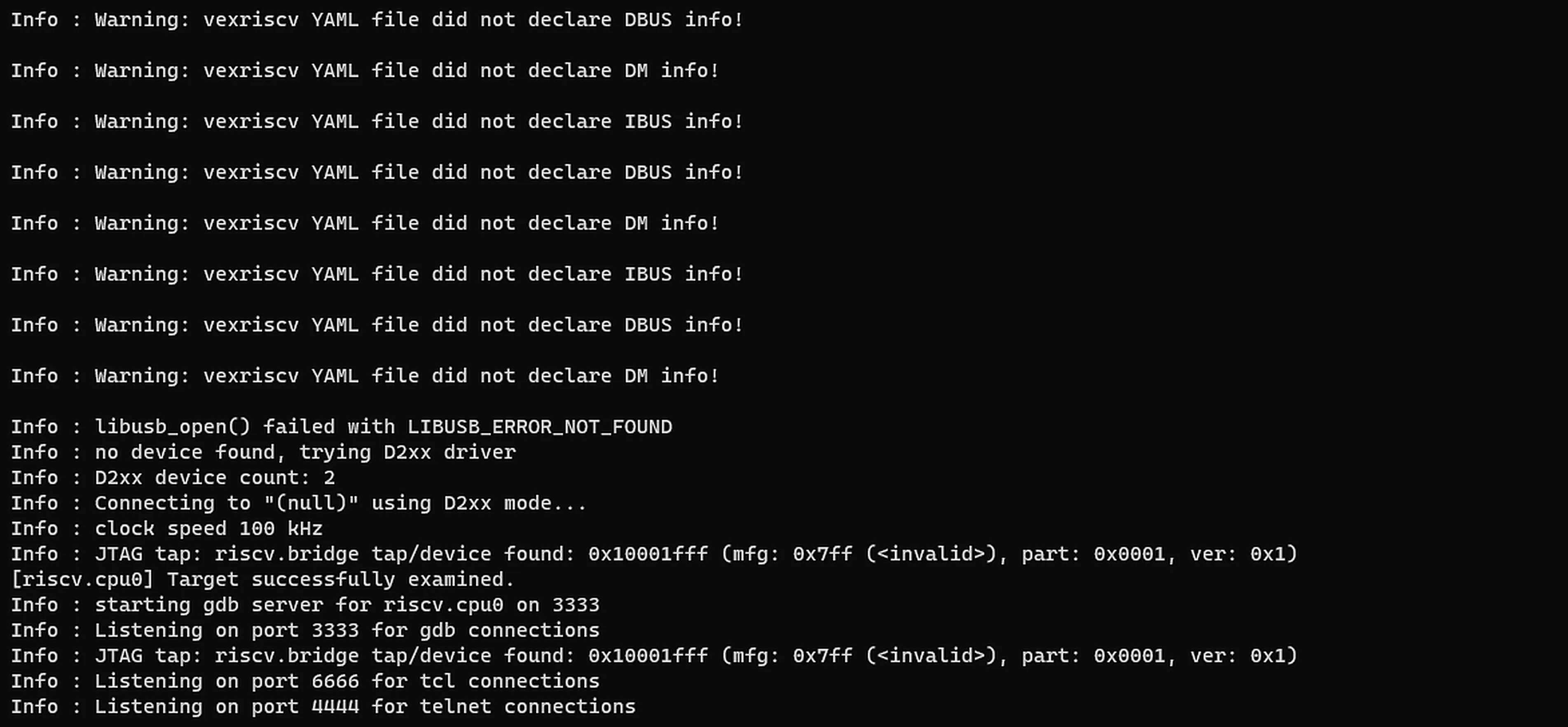
ECOS C3 chip supporting online JTAG debugging (Xiaoyu Hong)
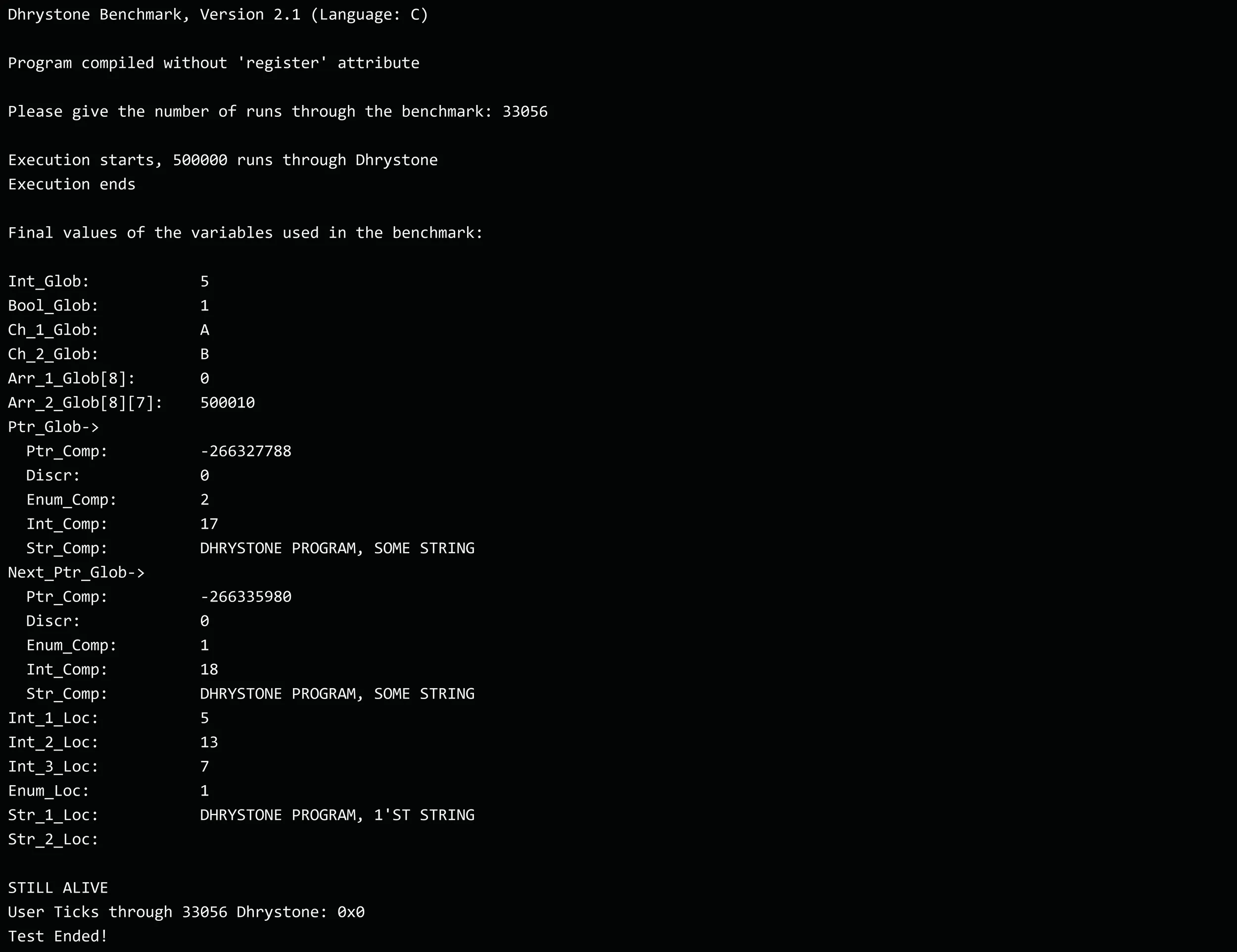
ECOS C3 running Dhrystone
The Tong Xiaojun team's chip test results were as follows: the basic clock signal operated normally (measured at 50.000002 MHz, with an error of approximately 0.000004%), and the IO_PAD68 (LCD_SPI_CLK) pin produced a clean square wave with compliant voltage levels and normal drive strength, verifying the basic power and timing behavior. Because the current tapeout version does not include a Flash controller, on-chip program bootstrapping has not yet succeeded. The team has defined a follow-up plan: load programs and verify functionality through external bootstrapping with an FPGA, using an SoC4 JLCPCB motherboard. The SoC4 motherboard design files are ready. After the board is fabricated, the team plans to build a complete test platform and conduct comprehensive tests of the AI accelerator's computing capability, power consumption, interfaces, and other key metrics.
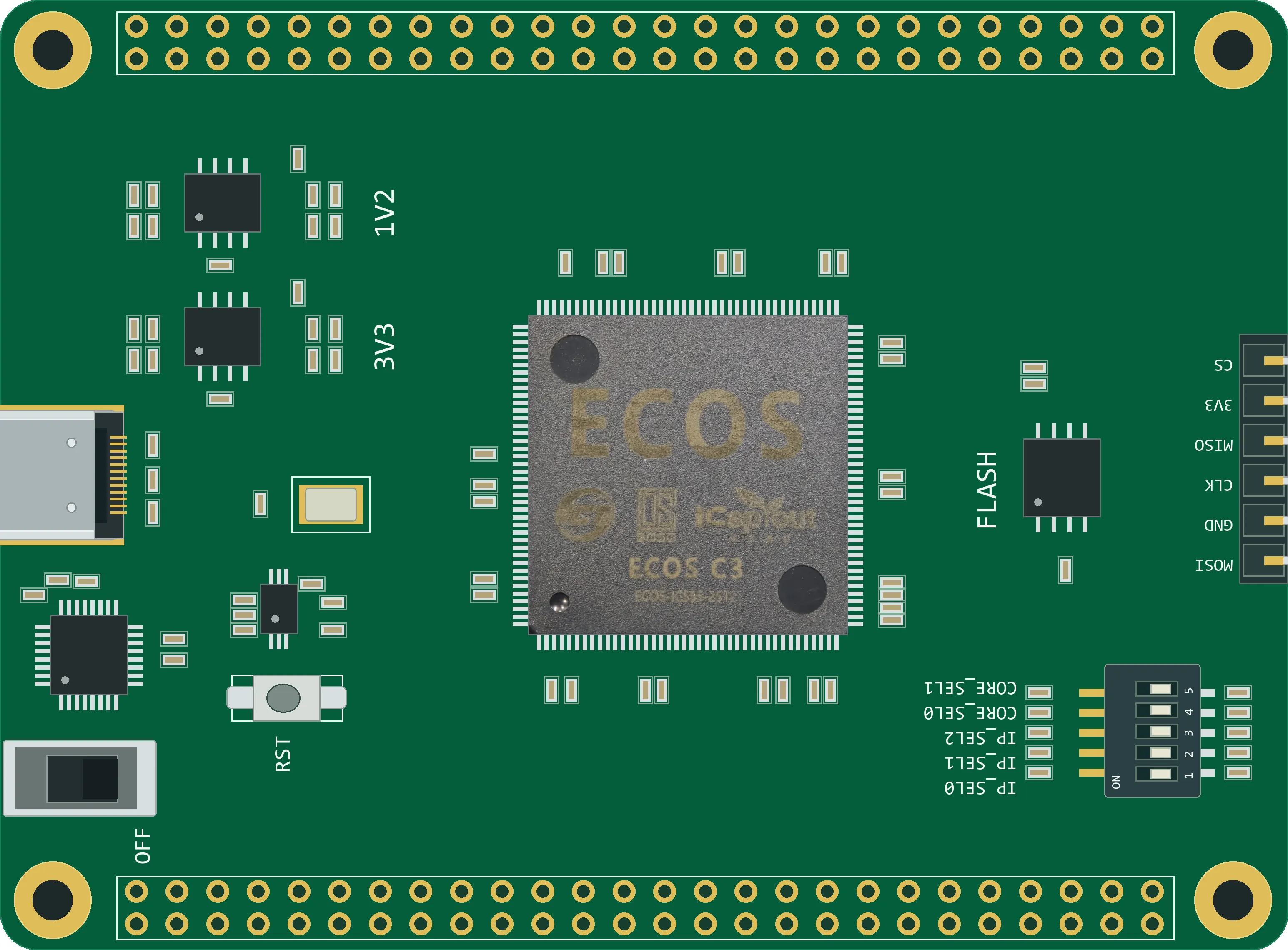
ECOS C3 chip board (Xiaojun Tong team)
The ECOS C4 chip was designed and tested under the leadership of the Fan Rong team, a community team. The chip has three major highlights. First, it includes the independently designed SC32 RISC-V control processor core. The core uses a five-stage pipeline and has a target clock frequency of 50 MHz. It can handle on-chip control, task scheduling, and software execution. Standard AXI interfaces connect it to peripherals such as the serial port, clock, and SPI Flash, forming a minimal runnable digital chip system. Second, it implements dedicated SM3/SM4 instruction extensions for cryptographic workloads. Hardware and software cooperate to improve the execution efficiency of Chinese cryptographic algorithms. Third, it implements an XIP (Execute In Place) boot mechanism. The processor core can fetch instructions directly from external non-volatile memory, providing a foundation for building a more complete cryptographic SoC.
The chip successfully produced SM3 encryption and decryption results during its first bring-up test, and all core functions operated normally! During the project, members of the Fan Rong team used the ICsprout 55nm open-source PDK and further built practical experience with process libraries, design-rule constraints, timing closure, and layout implementation, improving their ability to independently carry out digital IC design and engineering verification. The team also verified the implementability of its RISC-V processor, cryptographic instruction extensions, and boot mechanism on real silicon, completing the transition from FPGA and simulation verification to a physical chip platform. Going forward, the team will continue to improve the SC32 processor core, cryptographic instructions, and algorithm accelerators, while researching reconfigurable computing architectures for post-quantum algorithms such as Kyber and Dilithium. The goal is to accelerate the development of an independently controllable, scalable, and practical technology stack for post-quantum cryptography chips.
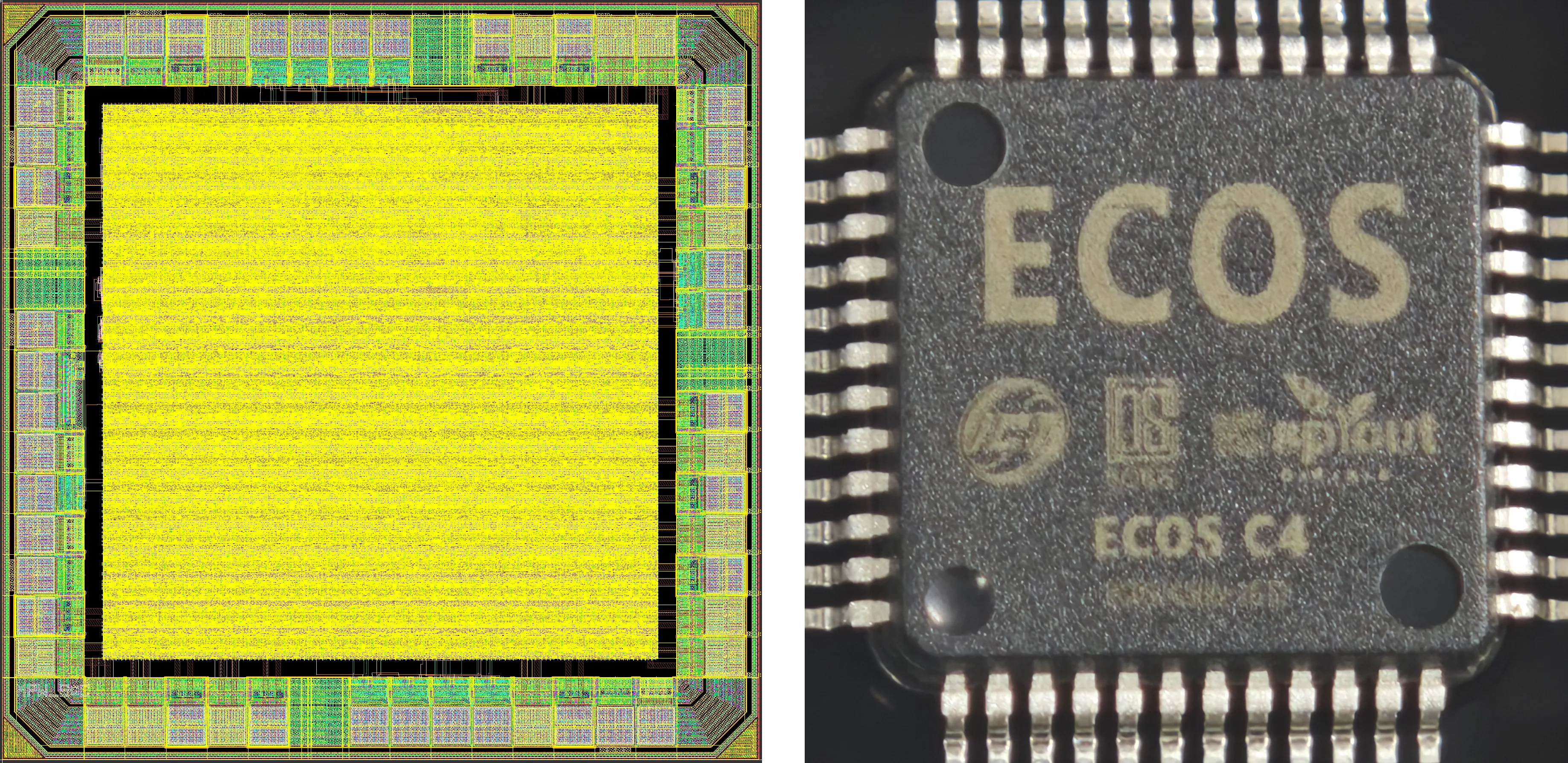
ECOS C4 chip (tapeout ID: SoC5)
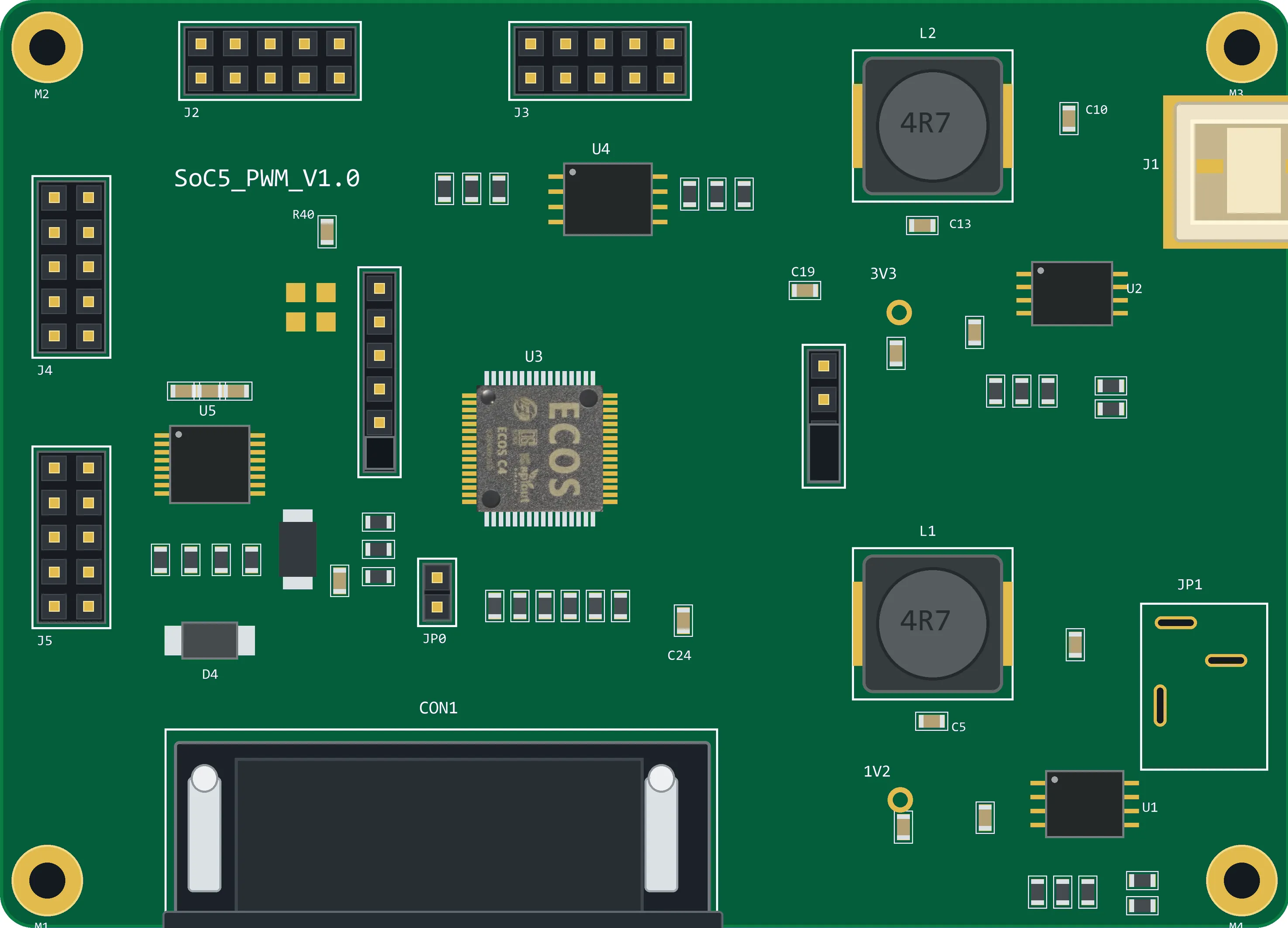
ECOS C4 chip board
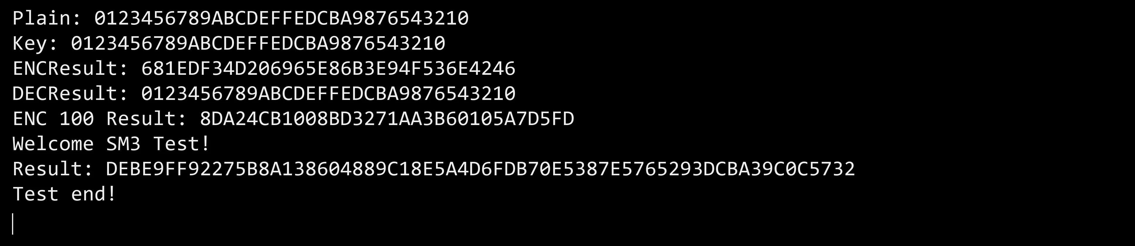
ECOS C4 chip outputting encryption and decryption results
03 ECOS Factory Open Source IP
The ECOS IP library is an important component of the ECOS Factory tapeout platform and will provide users with silicon-validated, directly integrable IP packages. The ICS55 macros are a series of foundry IP blocks developed by the ECOS Team using the ICsprout 55nm open-source PDK. They encapsulate complex analog, digital, or mixed-signal functions as standard macros and provide LEF, Liberty, Verilog models, and interface documentation for use in RTL simulation, logic synthesis, placement and routing, and other backend stages. Thanks to standardized interfaces, supporting models, and post-silicon validation, ICS55 macros eliminate the traditionally complicated foundry-IP development and adaptation process, significantly shorten chip design and verification cycles, and greatly improve the reusability of digital-circuit designs and tapeout success rates. All foundry IP except the DDR PHY has now completed post-silicon validation.
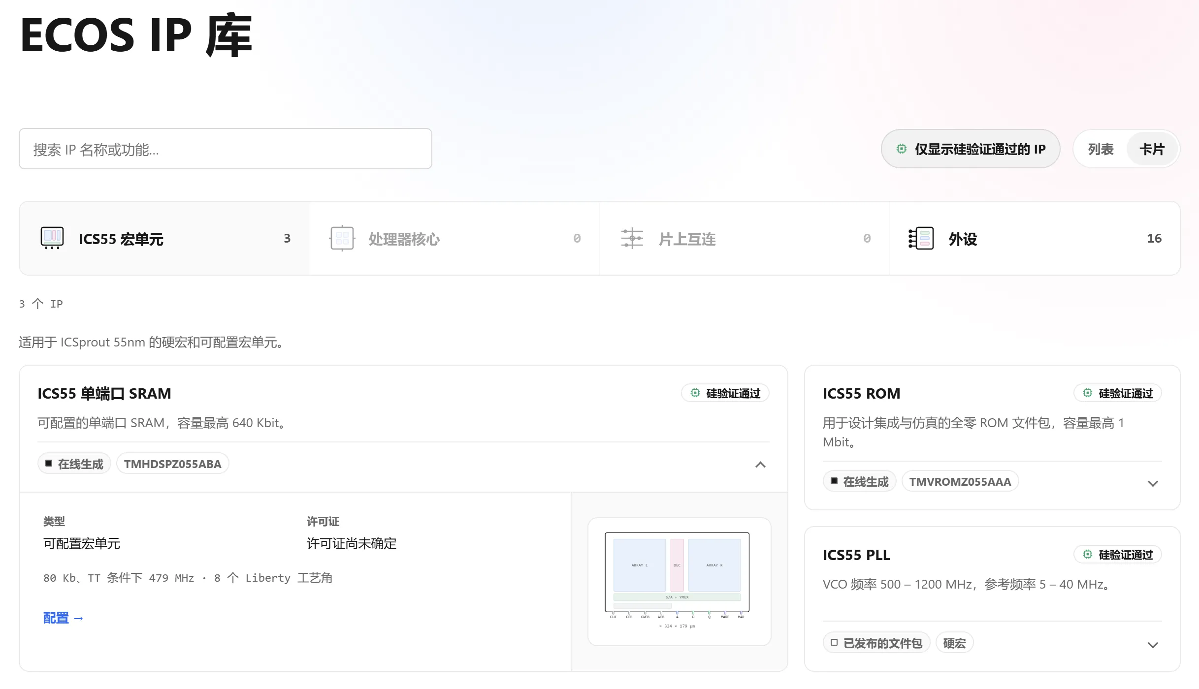
ECOS ICS55 macro library
The ECOS IP library provides the world's first SRAM Compiler for an open-source 55nm process (https://factory.openecos.com/ip/sram). It supports online configuration of synchronous single-port SRAM for the ICS 55nm process, with capacities up to 640 Kbit (80 KiB) and data widths from 2 to 160 bits. Users can set the memory specifications, implementation options, and interfaces as needed, then generate and download a package online. The ECOS Team has also introduced a macro preview feature to the Compiler for the first time, allowing users to view the configured SRAM macro's area, dimensions, frequency, power consumption, and other information in real time for early-stage selection. The ROM Compiler (https://factory.openecos.com/ip/rom) follows a similar process and supports online configuration of synchronous single-port ROM for the ICS 55nm process, with capacities up to 1 Mbit (128 KiB) and data widths from 4 to 128 bits. Note that the .romcode file in the package contains only zeros by default and can be replaced locally for simulation. For tapeout, specify the required ROM content replacement in the order comments; the ECOS Team will generate the corresponding layout.
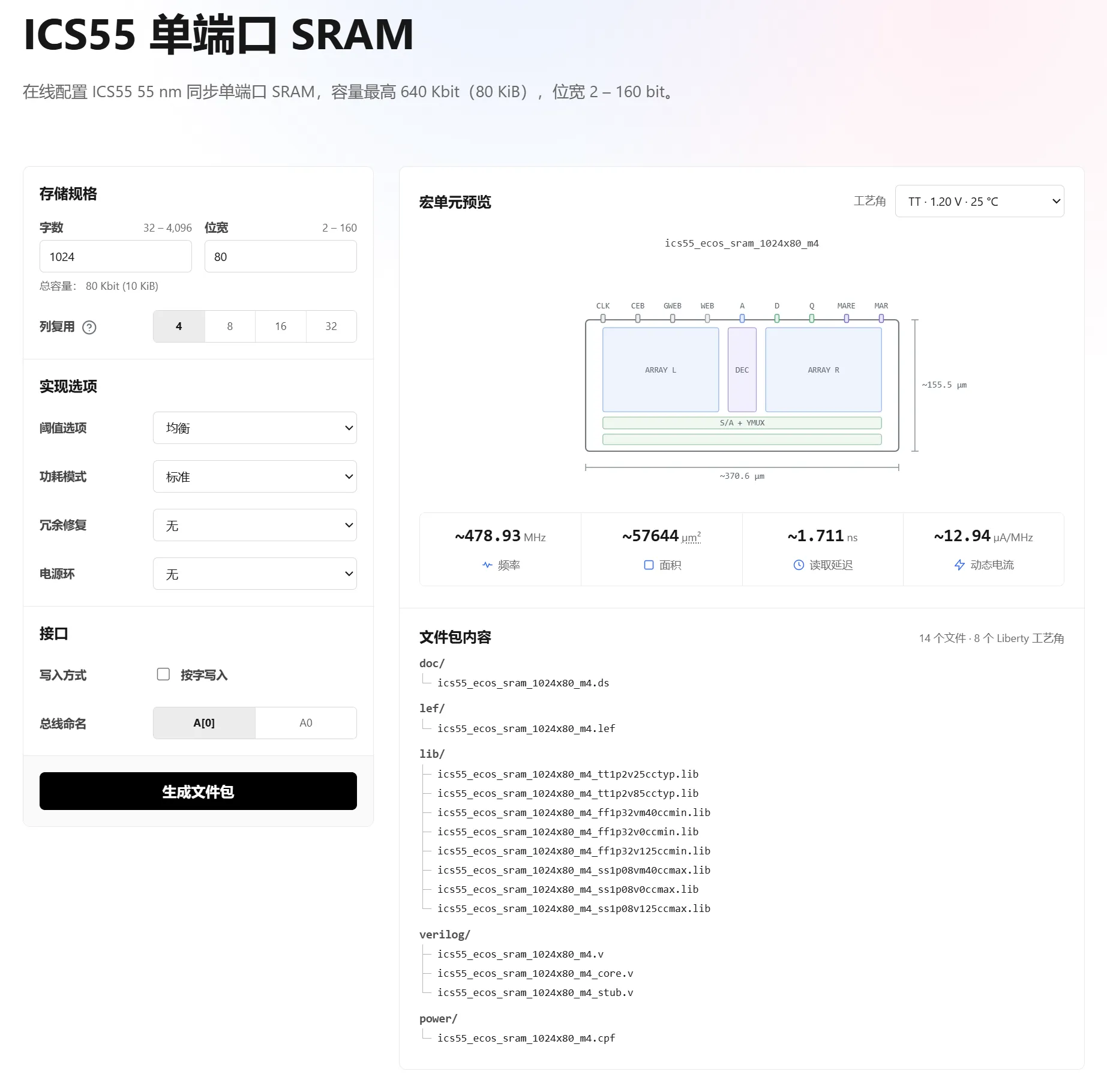
ICS55 SRAM online generator
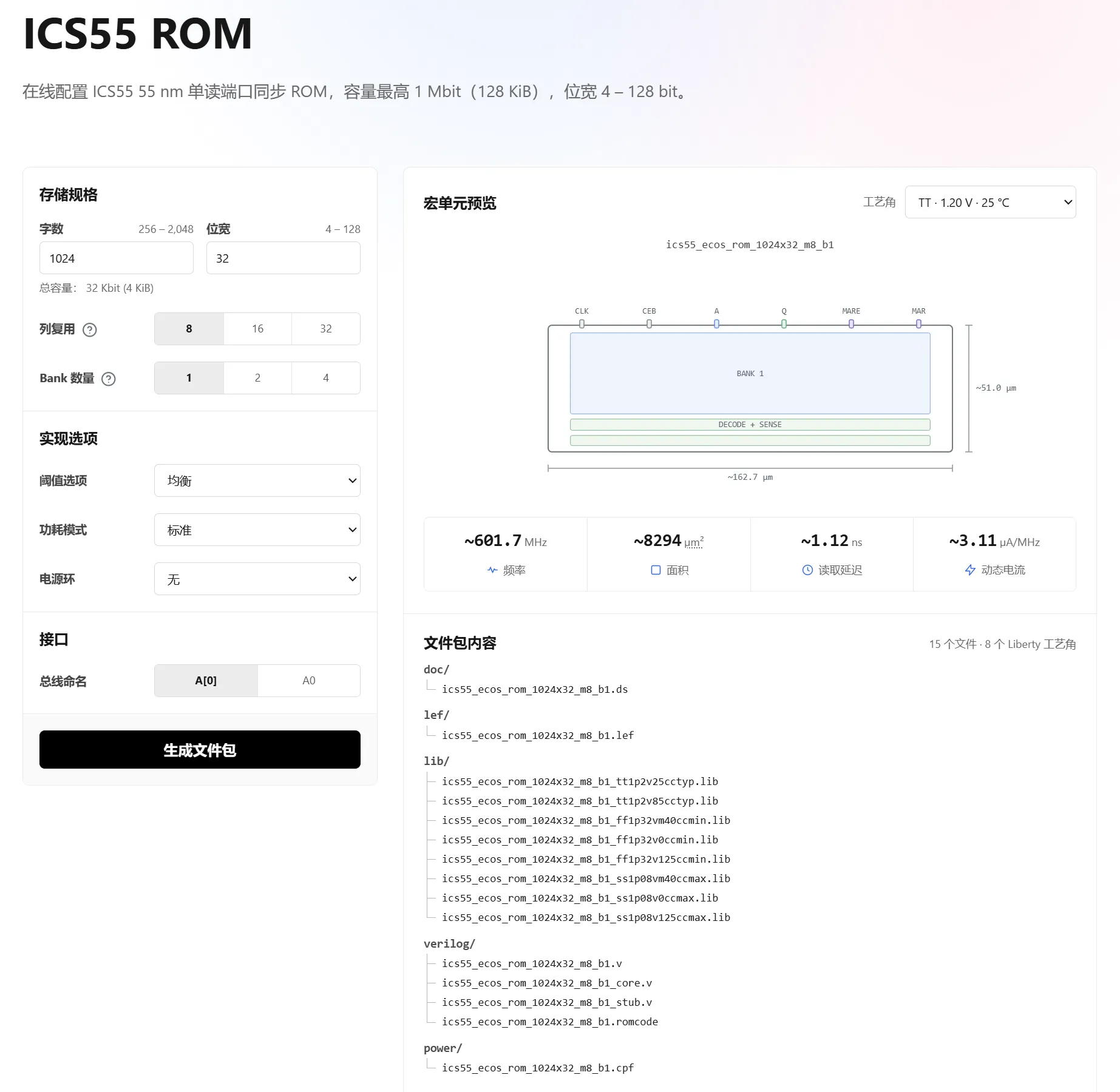
ICS55 ROM online generator
The PLL is an important IP block in digital-circuit design. Its main function is to convert an external reference clock into the high-frequency, multiple, or divided clocks required inside a chip. The ICS55 ECOS PLL (https://github.com/openecos-projects/ics55_ecos_pll) provides behavioral and black-box models, as well as LEF and Liberty views. It supports reference-clock inputs from 5 to 40 MHz and multiplied clock outputs from 500 to 1,200 MHz. The macro measures 200 μm × 120 μm and includes independent power connections for the analog, digital, and output-driver supplies. Normally, after users configure the PLL feedback divider, output divider, bypass, and enable parameters, the IP automatically generates the corresponding main and test clocks. The latest PLL updates are as follows: three Liberty corners (min/typ/max) have been added to cover different voltage and temperature conditions; the behavioral model has been updated for more complete functional simulation; and the README has been improved with interface definitions, power connections, LEF placement, and routing instructions.
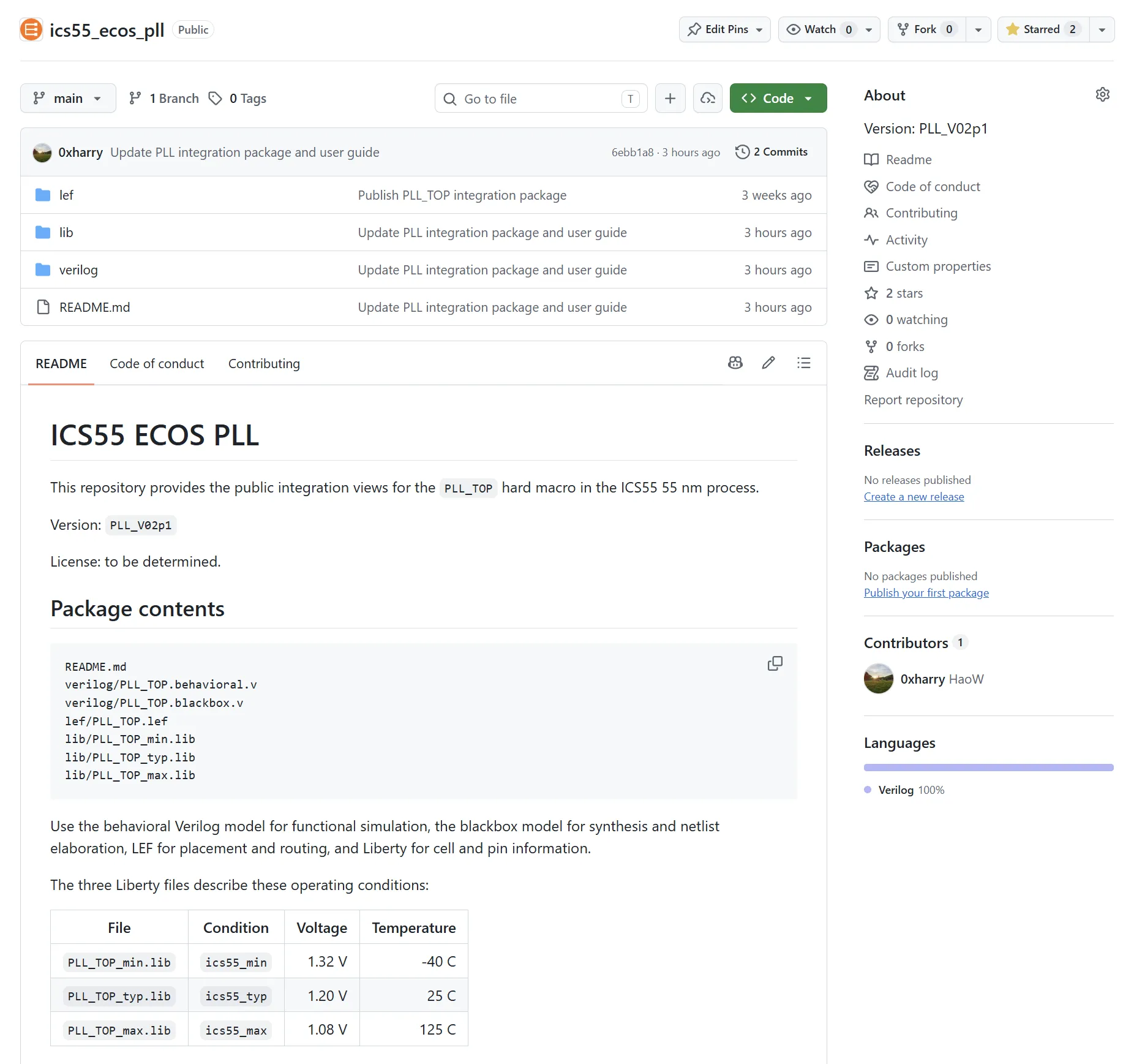
ICS55 PLL repository

ECOS tapeout discussion group
04 About the ECOS Team
The name ECOS comes from the initials of EDA, Chip, One Student One Chip, and System Solution, while also forming the first four letters of "Ecosystem." The ECOS Team includes members from the Institute of Computing Technology of the Chinese Academy of Sciences, the Beijing Open Source Chip Research Institute, and the open-source community. The ECOS Team focuses on fully open-source chip design solutions built on open-source EDA, open-source IP, and open-source PDKs. Its vision is to use open source to lower the barrier to chip design and empower a wide range of industries. To share the team's research with open-source chip enthusiasts, we created the Weixin account "ECOS开源芯片. It covers the latest developments in open-source IP/SoC, open-source EDA, open-source PDKs, embedded systems, design platforms, and community activities. Everyone is welcome to search for "ECOS开源芯片" on Weixin and follow us! The ECOS Team's website is openecos.com, and our contact email is ecos-all@ict.ac.cn. Please send any questions or suggestions to this address, and we will reply as soon as possible.
Original link: https://mp.weixin.qq.com/s/Io_Irm3AA88n9_BPjWcAjw