From Open Source Chips to AI Hardware: Highlights from the ECOS Team at the JLC Spark Conference
On September 19, the Shenzhen Convention and Exhibition Center in Futian was packed with visitors for the 4th JLC Open Source Hardware Spark Conference and Global AI Hardware Innovation Ecosystem Summit, hosted by JLC Group. The event attracted more than 2,200 engineers, makers, enthusiasts, industry experts, university faculty members, and students from countries and regions around the world. More than 50 industry partners also exhibited at the conference, showcasing the latest advances at the intersection of open-source hardware and artificial intelligence. The event created a platform for collaboration across the industry and opened a new chapter for the AI hardware innovation ecosystem.
As announced in our earlier article, "The ECOS Team Is Heading to the Spark Conference: Visit Our Booth and Explore Fully Open Source Chips", the ECOS Open Silicon Team (hereinafter the ECOS Team) joined the conference as a partner of the JLC Maker Fair. We brought our in-house open-source chips, development boards, robots, handheld game consoles, and chip design platforms to the event, presenting a range of achievements from across the open-source chip ecosystem. Visitors came throughout the day, from experienced embedded developers to students encountering hardware development for the first time. All showed strong interest in our vision of enabling everyone to design open-source chips.
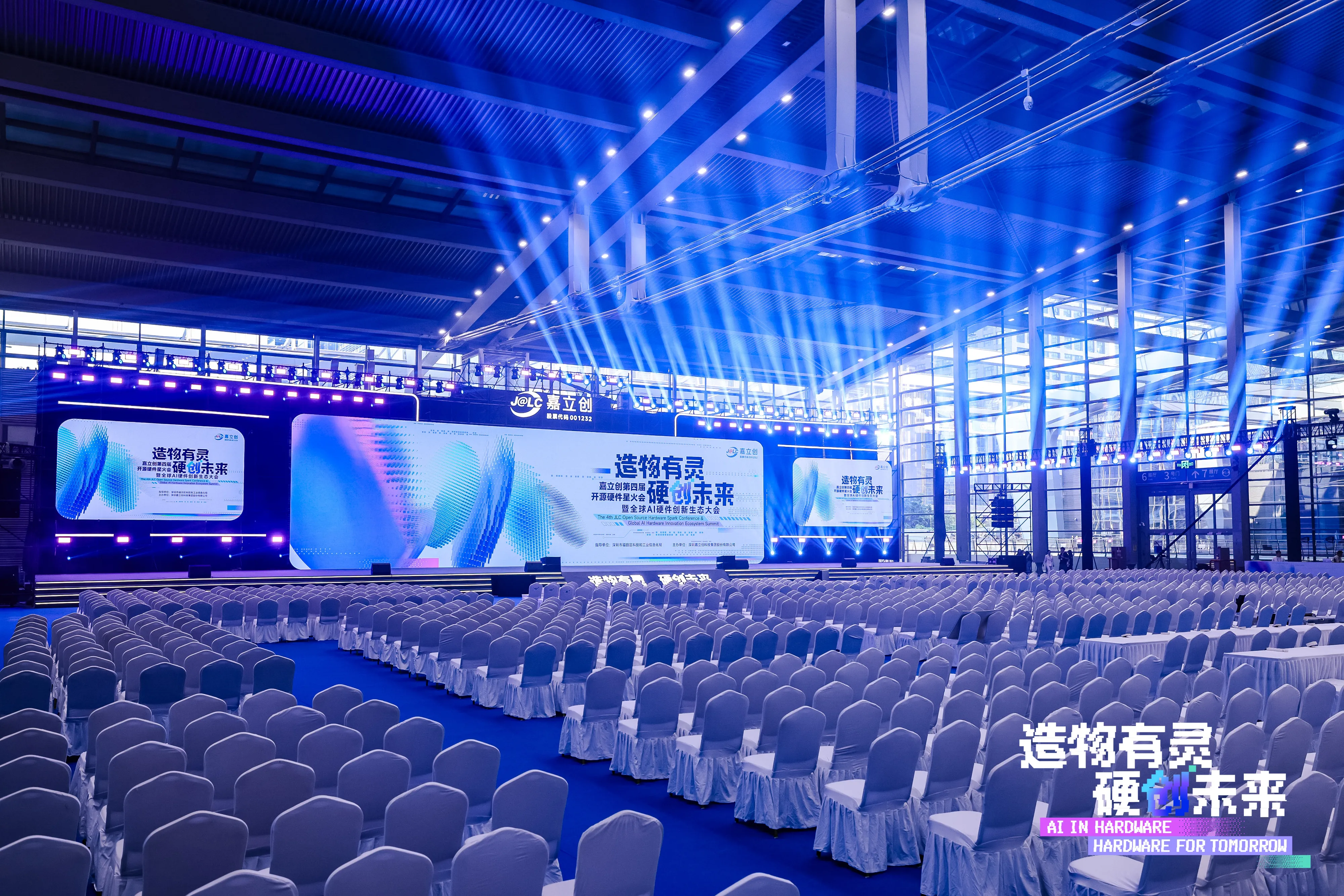
The JLC Open Source Hardware Spark Conference
01 Full Stack Open Source Chips and the PCB Soldering Competition
The ECOS Team showcased its 55nm open-source chips, StarrySky development boards (including boards for "One Student One Chip" and the 55nm open-source chips), the new XiaoXin Mambo Robot, the XiaoXin robotic arm, and the GameZero handheld game console. Visitors operated the robotic arm themselves and used voice commands to make the XiaoXin Mambo Robot perform a variety of entertaining movements, experiencing the appeal of a full-stack open-source chip platform firsthand. We also added a chip-layout demonstration on the spot. Embedded developers are already familiar with PCB layouts, so when we introduced the more complex and highly integrated chip layouts, they quickly grasped the concepts and expressed strong appreciation for our work on open-source chips.
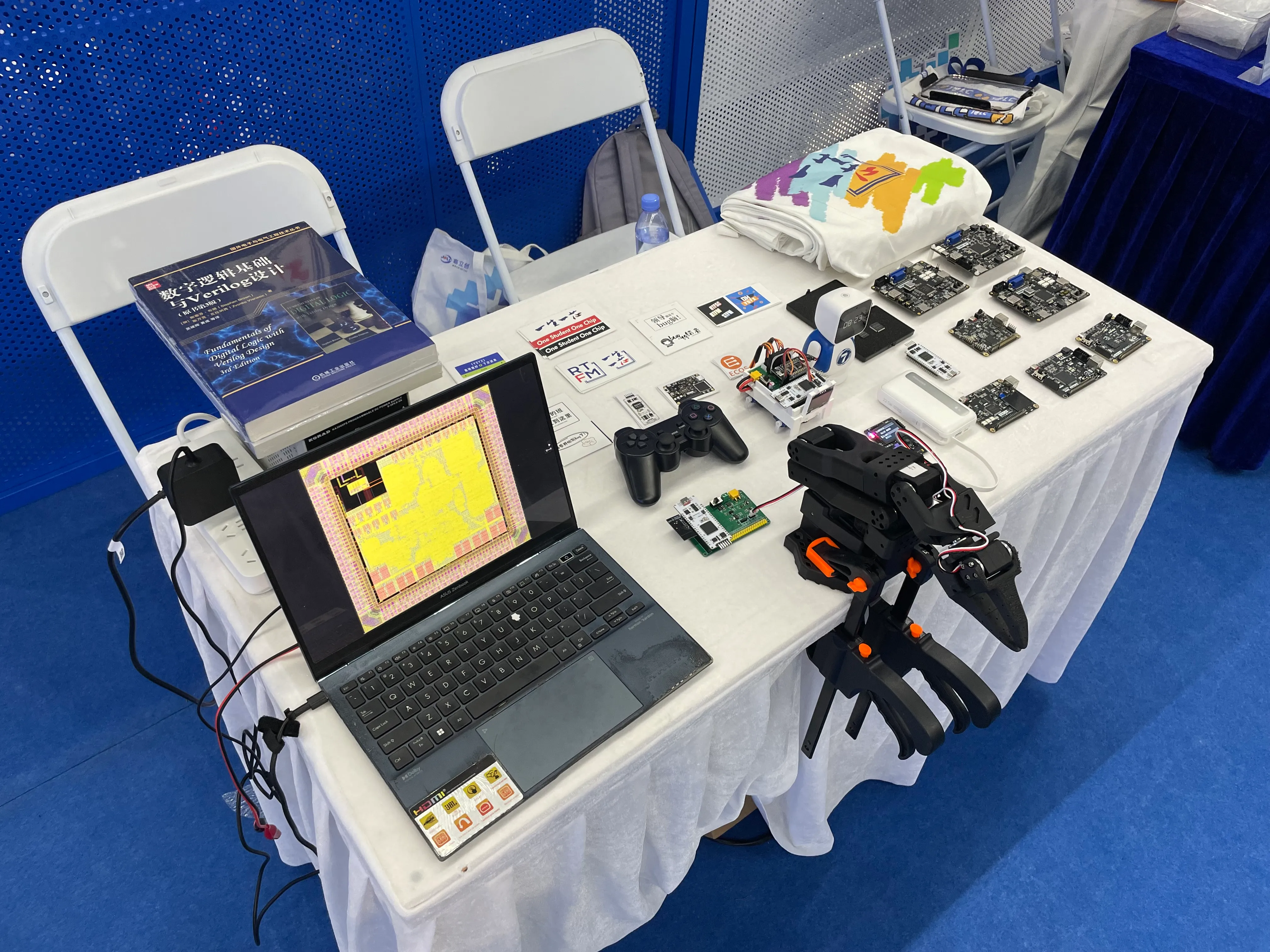
The ECOS Team's booth at the JLC Maker Fair
In addition to presenting at the exhibition, ECOS Team member Mingju Liu entered the hugely popular "Soldering Emperor" competition. One hundred soldering engineers competed side by side, with 100 soldering irons in operation at the same time. The scene resembled a martial-arts tournament created especially for hardware enthusiasts. The contestants worked in total concentration, carefully handling every pad as soldering-iron tips moved rapidly in their hands, and the tense, exciting atmosphere energized the entire venue. From chip design to hand soldering, ECOS Team members can write RTL at their desks and pick up a soldering iron to assemble a circuit board. This is the appeal of open-source hardware: from chips to boards and from design to implementation, people can participate directly in every stage.
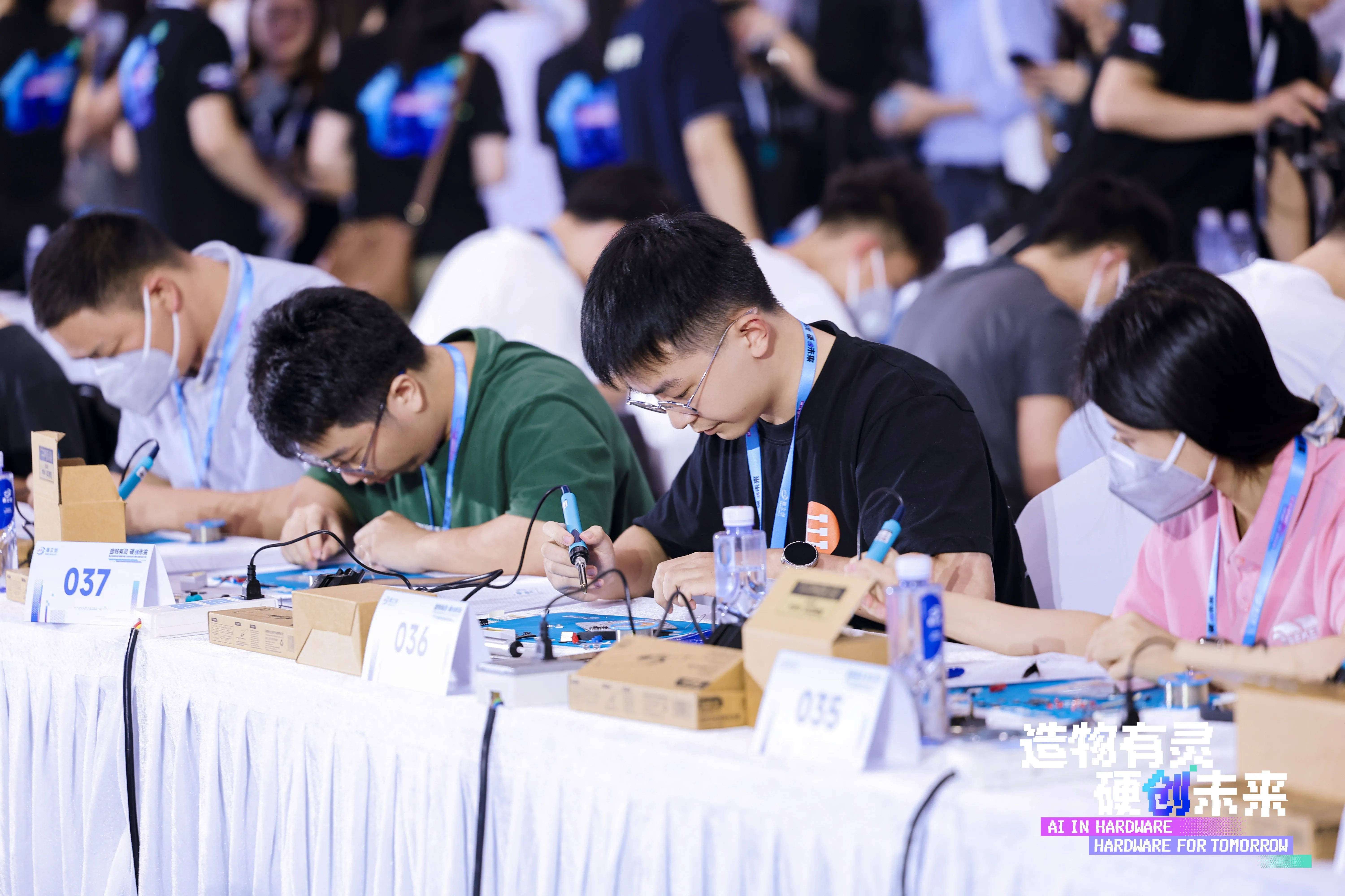
ECOS Team member Mingju Liu soldering a circuit board (the handsome contestant at center)
02 From Shenzhen to the Global Open Source Community
The ECOS Team's booth remained busy from the moment the exhibition opened until it closed. After seeing the team's latest tapeout results, many visitors asked about the details of our shuttle runs, including the design flow, tapeout costs, turnaround time, and toolchain. Our conversations with these embedded developers made it clear that they understand chip-design requirements better than almost anyone else. From the moment a chip is created, its ultimate purpose is to serve end users. Embedded developers build real-world solutions around chips, forming a vital bridge between chip designers and end users. Because they understand what users need, they have strong demand for chips that meet customized requirements. Low cost was another phrase we heard repeatedly. JLC has made PCB fabrication highly affordable, but chip tapeouts remain expensive. That reality is also the ECOS Team's greatest motivation for the work ahead.
We were also pleasantly surprised by the number of technically experienced visitors at our booth. Some had enrolled in the "One Student One Chip" program, while others were loyal followers who came specifically on the recommendation of open-source community influencer Wei Wu (our highest respect to lazyparser). With their technical backgrounds, these visitors wanted more than a close look at a physical 55nm open-source chip. They were also deeply interested in the processes and technologies behind the fully open-source chip design solution. Several asked specifically about the development of ECOS ChipCompiler, ECOS Studio, and ECOS Factory. They also discussed challenges they had encountered during chip design and tapeout with our team, giving us valuable insights.
Several engineers from industry visited the booth as well. They first expressed support for the ECOS Team's low-cost tapeout model and then offered valuable suggestions from a customer's perspective. One Shenzhen-based hardware engineer was particularly interested in two types of chips that he hoped future shuttle runs could support. The first would be similar to the MSPM0C1104 released by TI in March 2025. Its smallest package is an eight-ball WCSP measuring only 1.38 mm², which TI describes as the "world's smallest microcontroller." The device integrates 16 KiB of Flash, 1 KiB of SRAM, a 12-bit ADC, GPIO, and interfaces including UART, SPI, and I2C, making it highly attractive to consumer-electronics OEMs seeking ultra-low power and miniature system integration. The second would be a heterogeneous MCU+FPGA chip. Many users need to run software on an MCU while also using a certain amount of programmable logic. Combining the two, together with suitable tools and documentation, could create a highly competitive product.
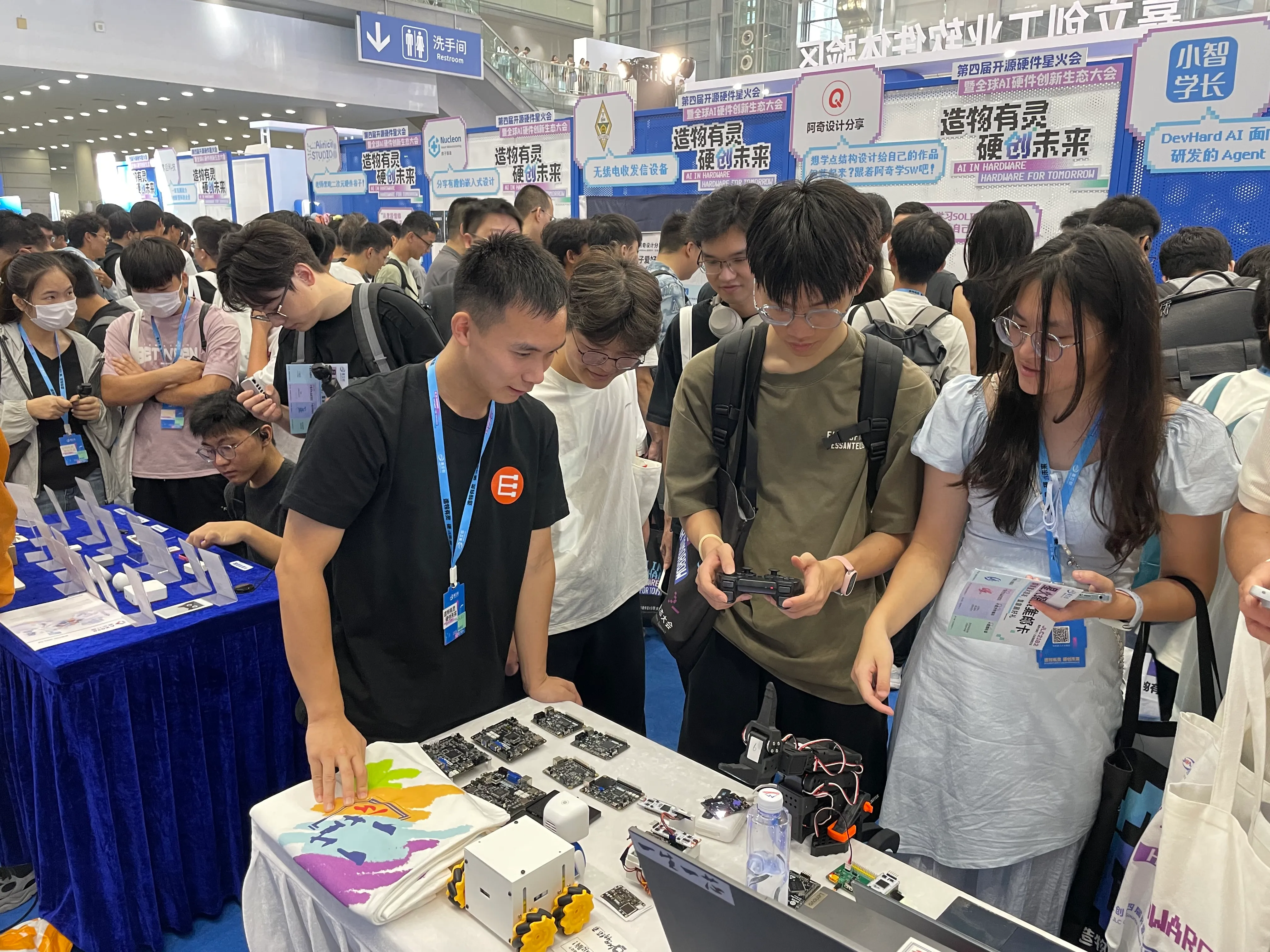
Chinese makers visiting the ECOS Team's booth
Shenzhen is a center for chip, embedded-system, and electronics enthusiasts from around the world, not least because of Huaqiangbei. Many international users closely follow the hackathons, maker fairs, and community events held in the city. Veteran Japanese maker Masakazu Takasu, who now lives in Shenzhen, attended this year's Spark Conference as a visitor. He had spoken at an earlier edition of the conference, where the author had the opportunity to meet him. When he reached the ECOS Team's booth, the exhibits quickly caught his attention. We briefly introduced the complete chip-design flow built by the ECOS Team around open-source EDA, open-source IP, and the ICsprout 55nm open-source PDK. When we explained that students who complete the "One Student One Chip" course can participate in an MPW tapeout free of charge and receive a chip of their own, he was astonished and asked us to confirm that he had correctly heard "55nm open-source PDK." After the event, Takasu published an article praising the ECOS Team's work: making custom chips is becoming the next stage on which Chinese makers can exercise their creativity.
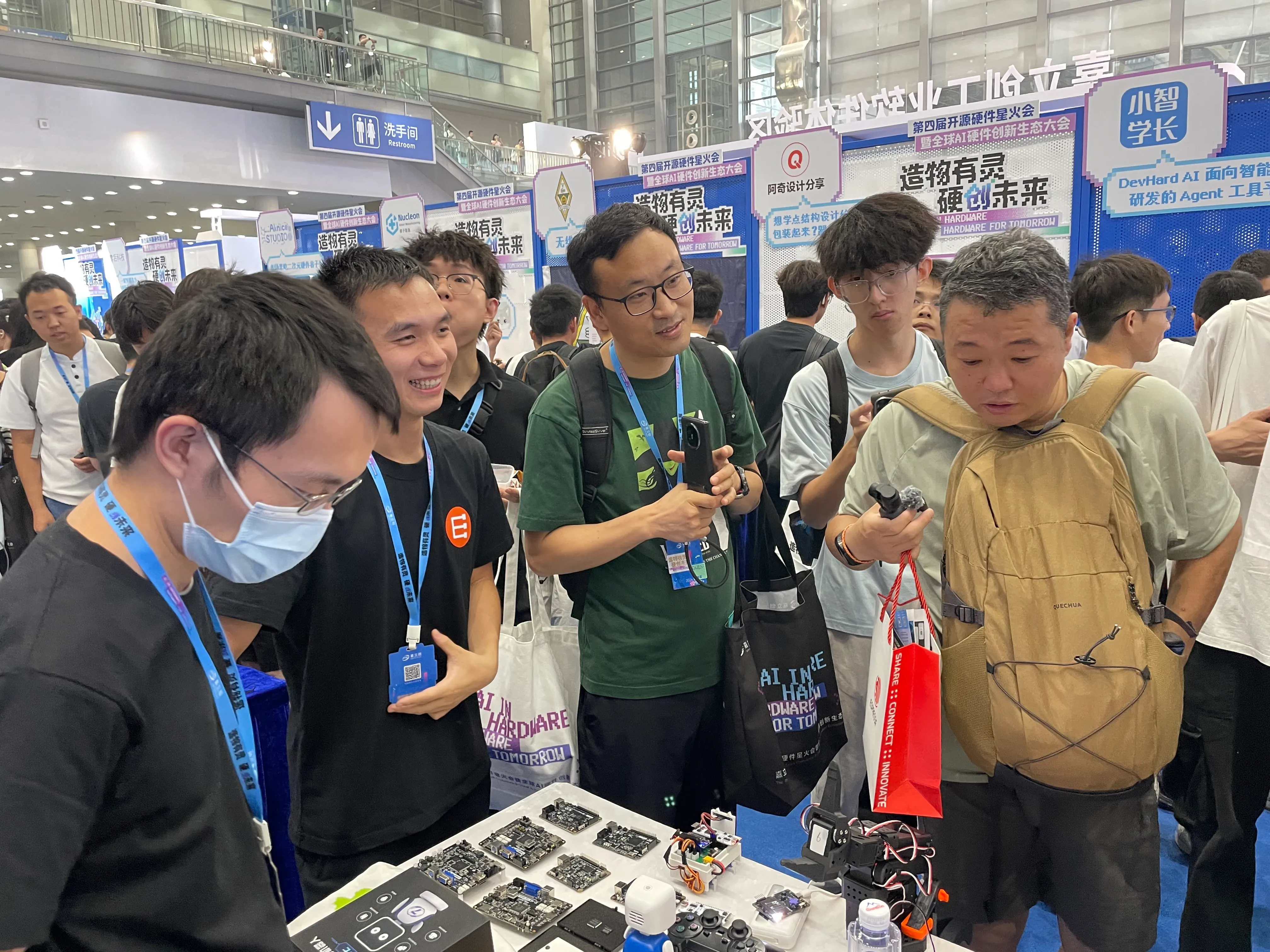
Veteran Japanese maker Masakazu Takasu (right) visiting the ECOS Team's booth
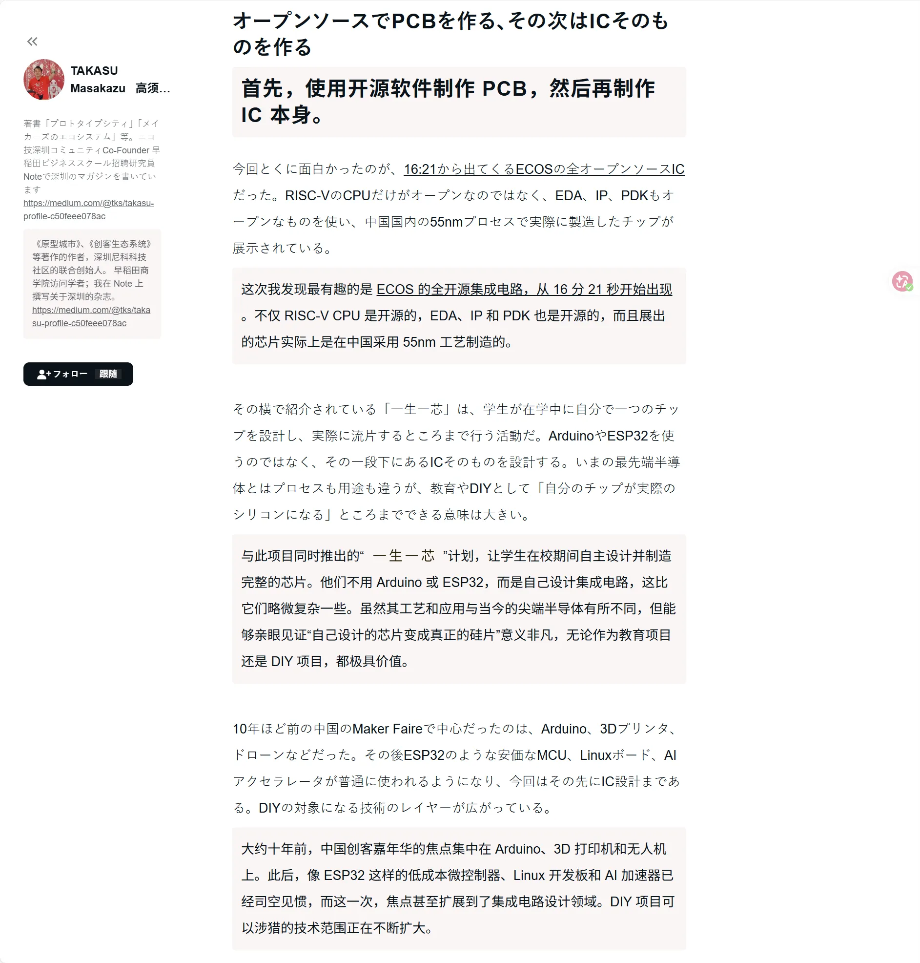
Masakazu Takasu highlighted the ECOS Team's fully open-source chips and the "One Student One Chip" program in his article
Another visitor from Japan, Junichi Akita, posted on X to introduce the ICsprout 55nm open-source PDK and the ECOS Team's "One Student One Chip" program to Japan's open-source community. Akita is a professor at Kanazawa University whose research covers integrated circuits, CMOS image sensors, interactive systems, and wearable computing. In addition to achievements in smart image sensors, tactile sensing, and conductive-fabric networks, he has long promoted MakeLSI:, an open-chip project dedicated to lowering the barriers to chip design and tapeout. As an active maker, he regularly participates in electronics projects and events related to chips, exploring complete open-source solutions that extend from low-level chip design to human-computer interaction. His post from this year's Spark Conference recognized the ECOS Team's achievements and carried the open-source chip spirit into another community.
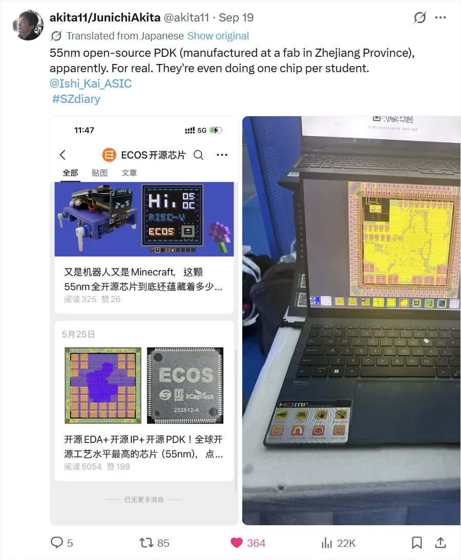
Kanazawa University professor Junichi Akita posted about the 55nm open-source PDK and the "One Student One Chip" program on X
03 Reflections After the Spark Conference
JLC was officially listed on the Shenzhen Stock Exchange in August this year. On the day of the listing, Professor Yungang Bao published an article titled "The RISC-V Sector Needs the JLC Model," in which he summarized three defining characteristics of the JLC model. First, it focuses on long-tail users. According to figures announced at this year's Spark Conference, the JLC cloud platform has accumulated more than 10 million registered users, including 7.3688 million users of JLC EDA worldwide, while its open-source community has received more than 40,000 project submissions. These long-tail users, once overlooked by traditional PCB companies, helped JLC open a vast market worth billions to tens of billions of yuan in revenue. Second, it delivers low costs. Attracting long-tail users depends on reducing costs and improving efficiency. Through smart panelization and a series of other innovations, JLC has substantially reduced PCB fabrication costs while also shortening delivery times. Third, it enables agile development. With five digital production bases, JLC has connected the entire PCB design and manufacturing flow so that every stage works together seamlessly. It has even introduced AI Agent technology into the latest version of its EDA software, aiming to build an end-to-end PCB ecosystem for the AI era and help users iterate, manufacture, and deliver products faster.
Can the JLC model be replicated? The answer is yes. Even before this year's Spark Conference, the ECOS Team had learned through multiple channels that users in China and overseas have enormous demand for customized chips. They are the long-tail users of the chip industry. The ECOS Team has also opened a series of IP modules, including SRAM and PLL, and built ECOS Studio, a local integrated development environment for agile chip design, around the ECOS ChipCompiler open-source EDA toolchain and the ICsprout 55nm open-source PDK. At the right time, we also launched ECOS Factory, a cloud platform for MPW aggregation and tapeout that can significantly reduce the sunk costs incurred during the early stages of chip design. Finally, AI Agent technology will make conventional chip-design flows increasingly efficient. For tapeout, the author believes that agile manufacturing is not an unrealistic idea. A new manufacturing model for fragmented design requirements will eventually emerge, allowing users to receive chips of their own design in less time and establishing an open-source chip ecosystem built around rapid experimentation, rapid evolution, and rapid deployment.
Sparks gather, and open source gains momentum. The ECOS Team has always believed that chip design does not have to remain out of reach. We are continuing along the path that JLC once traveled. It may still be too early to say that everything is ready except for the final push, but the ECOS Team's previous tapeouts have already demonstrated one point convincingly: we are moving in the right direction. Finally, we sincerely thank everyone who visited the ECOS Team's booth. Your enthusiasm made the day especially meaningful. See you at the next Spark Conference!
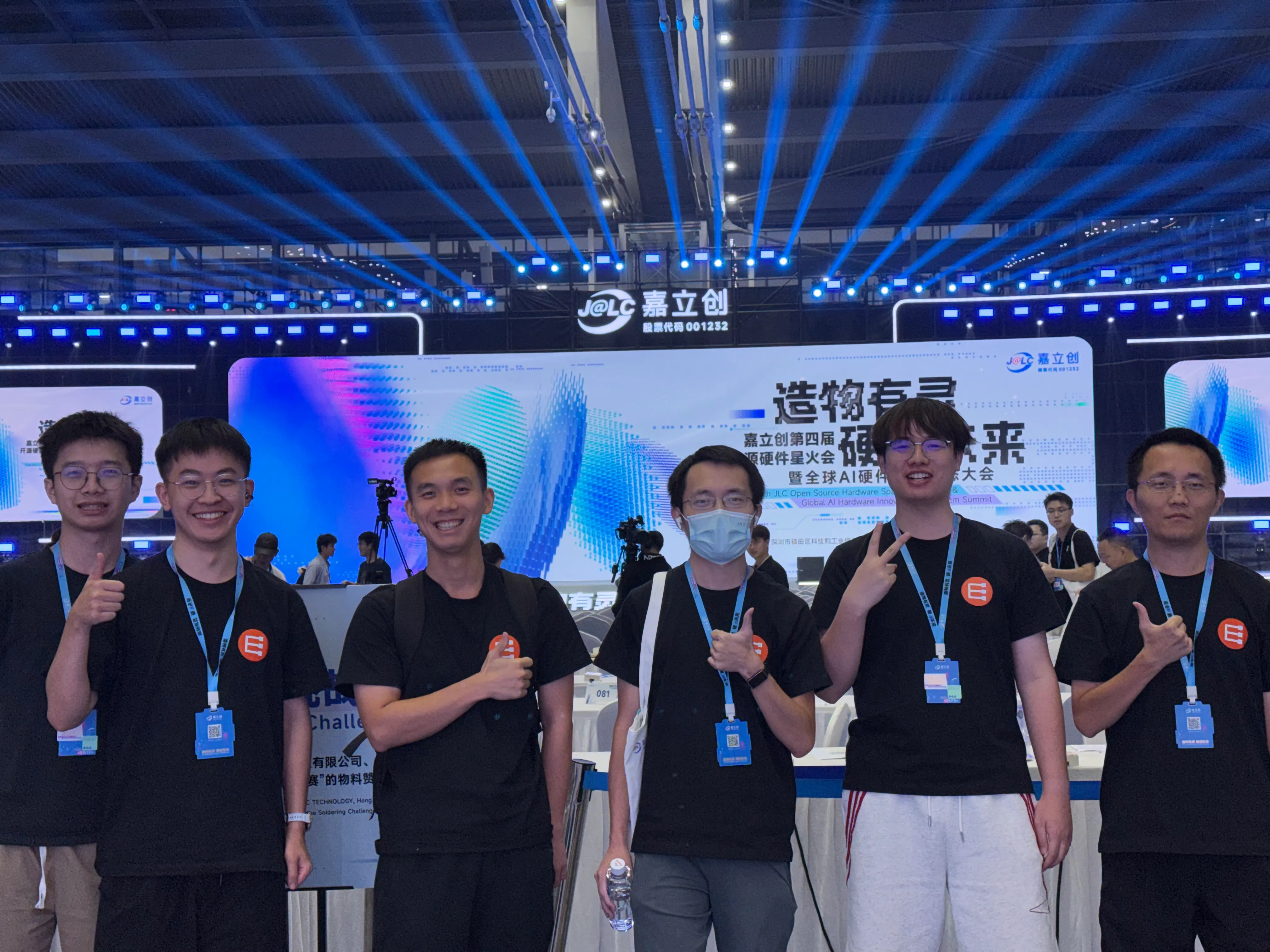
ECOS Team group photo at the Spark Conference
Original link: https://mp.weixin.qq.com/s/5UHSUXOO_LDAU131gQCN5Q