Skip to content

ICsprout

From Open Source Chips to AI Hardware: Highlights from the ECOS Team at the JLC Spark Conference
On September 19, the Shenzhen Convention and Exhibition Center in Futian was packed with visitors for the 4th JLC Open Source Hardware Spark Conference and Global AI Hardware Innovation Ecosystem Summit, hosted by JLC Group. The event attracted more than 2,200 engineers, makers, enthusiasts, industry experts, university faculty members, and students from countries and regions around the world. More than 50 industry partners also exhibited at the conference, showcasing the latest advances at the intersection of open-source hardware and artificial intelligence. The event created a platform for collaboration across the industry and opened a new chapter for the AI hardware innovation ecosystem.

As announced in our earlier article, "The ECOS Team Is Heading to the Spark Conference: Visit Our Booth and Explore Fully Open Source Chips", the ECOS Open Silicon Team (hereinafter the ECOS Team) joined the conference as a partner of the JLC Maker Fair. We brought our in-house open-source chips, development boards, robots, handheld game consoles, and chip design platforms to the event, presenting a range of achievements from across the open-source chip ecosystem. Visitors came throughout the day, from experienced embedded developers to students encountering hardware development for the first time. All showed strong interest in our vision of enabling everyone to design open-source chips.
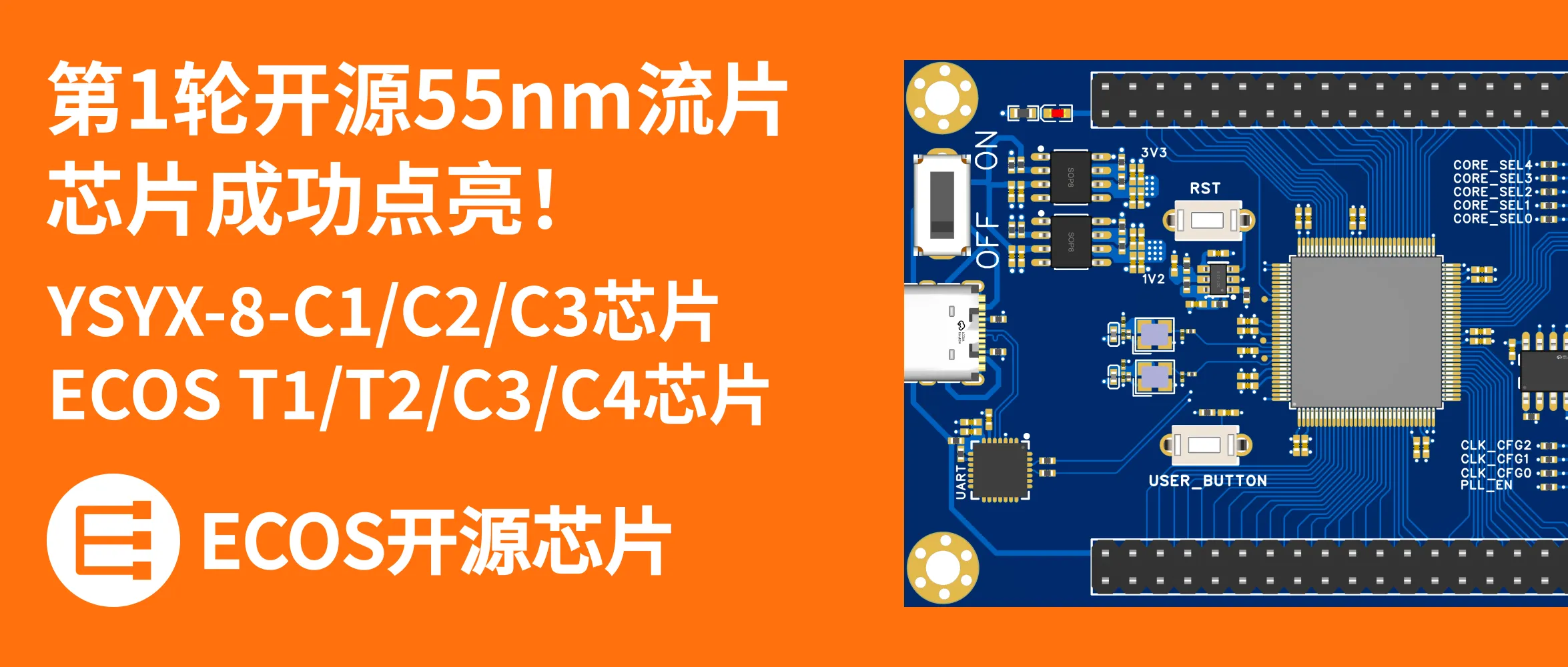
First Round Open Source 55nm Tapeout Results: Multiple Chips Successfully Brought Up!

The ECOS Team and community users conducted comprehensive testing of the chips from the first open-source 55nm shuttle run, and several chips were successfully brought up. This marks the ECOS Team's transition from a solution that primarily served its own chip designs to an open platform that supports different types of users in developing small-batch chips, based on open-source EDA, open-source IP, and an open-source PDK.

ICsprout 55nm Open Source PDK Officially Released!

The ECOS Team is proud to announce the official release of the world's first open-source PDK based on 55nm process technology! We are deeply grateful to ICsprout for contributing the world's most advanced, tapeout-ready open-source PDK at the time of release, marking a significant milestone in the history of open-source chips (glory to ICsprout). The open-source nature of ICsprout 55nm Open Source PDK (hereinafter referred to as this PDK) completely changes the high-barrier, high-cost predicament of traditional chip design. It provides universities, research institutions, and the open-source community with a complete pathway from chip design to tapeout manufacturing through open sharing, enabling researchers and developers to transform their imaginative design ideas into actual physical silicon wafers. Furthermore, thanks to the advanced nature of the 55nm process node in the open-source chip field, the complexity and flexibility of future open-source chip design will significantly increase, providing strong support for promoting the construction of the open-source chip ecosystem and the cultivation of chip talent.